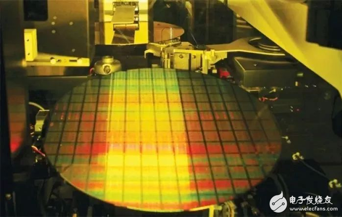
Daily Science News Featured Content preview “Mining Machine†started and Bitmain re-issued AI terminal chip to focus on security Large-scale organizational adjustment: Intel's manufacturing business will be divided into three Samsung 7nm LPP officially arrives, the world's first EUV lithography process Nearly 1 billion Lingang land acquisitions, Tesla's Shanghai super factory has a "safe place" ZTE and China Telecom complete the first 5G end-to-end full-service communication Bitmain releases AI terminal chip again, focusing on security On October 17, Bitmain officially released the terminal artificial intelligence chip BM1880, along with the Fortune Smart Server SA3 based on the cloud artificial intelligence chip BM1682, the embedded AI mini machine SE3, the 3D face recognition intelligent terminal and the BM1880-based intelligent terminal Development boards, AI modules, computing power sticks and other products. Tang Weiwei, Director of Product Strategy at Bitmain, said that Bitmain's cloud artificial intelligence chips are rapidly iterating at a rate of 9 months. Chip-based related products have performed well in actual operation. Customers have given positive feedback. Cooperation is being widely carried out, and many security projects continue to land. . At the same time, since the target market applications require AI solutions that integrate end-to-cloud, in order to better meet the needs of customers and the market, we decided to develop and launch end-side AI chips and solutions. The BM1682 chip was released in mass production in the first quarter of 2018, with a peak computing power of 3TFlops and a power consumption of 30W. It is the second-generation artificial intelligence chip launched by Bitmain for the field of deep learning. Large-scale organizational adjustment: Intel's manufacturing business will be divided into three According to reliable sources from foreign media, Intel’s technology and manufacturing business will be split into three different departments. It is reported that Sohail Ahmed, the director of the Intel Technology and Manufacturing Division, will leave next month, and he will be responsible for this position from 2016. After that, the Intel Technology and Manufacturing Division will be divided into three: The first is Technology Development. The person in charge is CTO Mike Mayberry, who was originally the director of Intel Labs. This position will be temporarily replaced by Rich Uhlig; the second is Manufacturing and Operations, the person in charge is Ann Kelleher; The third is the Supply Chain. The person in charge is Randhir Thakur. Obviously, Intel hopes to divide the complex process business into three relatively independent parts, responsible for R&D, manufacturing, and supply, with clearer responsibilities. Samsung 7nm LPP officially arrives, the world's first EUV lithography process Foundry Samsung announced that it has officially started using its 7nm LPP process to produce wafers. Samsung's 7-nanometer LPP process uses extreme ultraviolet lithography (EUV) technology, which will enable Samsung's 7-nanometer LPP process to significantly increase the transistor density in the chip while optimizing its power consumption. In addition, the use of EUV technology can also enable customers to reduce the number of photomasks required for each chip, and while reducing production costs, it can also shorten their production time. Samsung said that under the same complexity, the 7-nanometer LPP process can reduce chip area by 40%, reduce power consumption by 50%, and increase performance by 20% compared with the previous generation of 10-nanometer FinFET process. In addition, in terms of production costs, because the 7-nanometer LPP process has added EUV technology, when the silicon wafer is exposed at a wavelength of 13.5nm, compared to the traditional argon fluoride (ArF) immersion that uses a wavelength of 193nm for exposure in the past Technology, EUV technology only needs a single photomask to complete the exposure of a single-layer silicon wafer, while traditional ArF requires four photomasks to process. Therefore, the 7-nanometer LPP process not only reduces production costs, but also shortens production time. Nearly 1 billion Lingang land acquisition , Tesla Shanghai "settles down" On October 17, Tesla officially announced that the company and the Shanghai Municipal Planning and Land Resources Administration have formally signed a "Land Transfer Contract", and the scale of Tesla's Shanghai Super Factory will exceed 1,200 acres (over 860,000 square meters). Tesla said that Tesla had previously announced that it was accelerating the construction of the Shanghai Super Factory, hoping to learn from the experience of the continuous increase in North American Model 3 production capacity and build the Shanghai factory into a factory with high capital efficiency and rapid progress. The signing of the "Land Transfer Contract" is a solid step to achieve this goal. ZTE and China Telecom completed the first 5G end-to-end full-service communication On the morning of October 18, ZTE announced that it had cooperated with China Telecom to realize the first 5G field end-to-end full-service communication in Xiongan New Area. The test is based on the 3GPP R15 standard, using the 3.5GHz frequency band and SA networking architecture. This full-service integration marks another step forward for both parties towards large-scale commercial use of 5G in 2020. ZTE introduced that it provided commercial-oriented 5G end-to-end system solutions for this test, including 5G wireless base stations, core networks, bearers and terminal prototypes. The solution is based on the 3GPP R15 SA version, and the two parties jointly demonstrated 5G 4K high-definition video calls and 5G VR high-definition video services.
A membrane switch (PCBA), just like an electrical switch, turns the circuit on and off. These controls are slightly different from standard mechanical switches; however, the physics is the same.
When the two poles come in contact, the circuit closes, and the current flows. Nevertheless, Membrane Switches are advantageous because they are eco-friendly. Membrane switches are of many different types,
Pcba Membrane Switches,Pcba Membrane Switches And Outlets,Pcba Membrane Switches Keypad,Buttons Pcba Membrane Switch KEDA MEMBRANE TECHNOLOGY CO., LTD , https://www.kedamembrane.com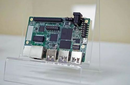
Tactile membrane switch
Non-tactile membrane switches
Mixed panels