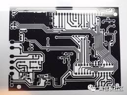
Now officially cut into the manufacturing process of the circuit board. Some people may say that you are not explaining the circuit board design. One is designing. Why does it take so much effort to introduce the circuit board process? This is because both the circuit design and the circuit board design are serviced for the purpose of subsequently producing a good circuit board and realizing the value of its development and mass production. If we regard production failure as a good opponent, then we should have a good understanding of our opponents. Do you know yourself. (1) Drawing Films Laser photo plotters are used to make films necessary for manufacturing processes such as wiring films, solder mask films, and printing films. Figure 9 shows the wiring film. In the process of sticking the film, there will be some errors, especially for special plates, the error will be greater. So in the circuit board design should fully consider the impact of these errors, make a suitable design. (2) Production of Cut-out Plates The size of the boards used to manufacture circuit boards is usually 1m by 1m or 1m by 1.2m. According to the need of production, the workpieces are cut into different work pieces, and the size of the designed circuit board is used to select a predetermined work piece size, thereby avoiding waste and increasing unnecessary costs. (3) Formation of inner layer circuit Next, the inner layer circuit wiring (1-5 of FIG. 2) is formed. Attach a dry film with light to a double-sided copper plate as an inner layer, and then stick the film used to make the inner layer, expose it, and perform the development process, leaving only the traces. Where needed. Both sides of the project are to be carried out by removing the unwanted copper foil by etching (Etching) devices. Figures 1 to 5 (4) Oxidation treatment (blackening treatment) Before the synthesis with the outer layer, the copper foil is subjected to oxidation treatment to form a fine uneven surface. This is to increase the contact area between the prepreg and the inner layer with insulation and adhesion, so that the adhesion is better. Today, in order to reduce environmental pollution, alternatives to oxidation treatment have been developed, and today's circuit boards have good contact with themselves. (5) Lamination Lamination As shown in FIG. 8 (6), the oxidation-treated inner layer circuit is covered with a semi-curing agent, and an outer copper plate is attached. In a vacuum state, the laminate is compressed while being heated. The semi-curing agent plays a role of blocking and insulating. After lamination, the appearance of the double-sided copper board looks the same, and the subsequent work is the same as that of the two-sided copper board. (6) Open hole CNC machine tool to open hole. (7) Removal of residue The heat generated when the hole is opened causes the filler to melt and adhere to the inner wall of the plated hole. It can be removed by a chemical agent to make the inner wall smooth and increase the reliability of copper plating. (8) Copper Plating The inner and outer layer connections need to be treated by copper plating. The first is electroless plating to form a minimum thickness capable of flowing current. Second, in order to achieve the plating thickness required for the design, electrolytic plating treatment is performed. The outer layer of copper foil is also plated with copper. The thickness of the outer layer is the thickness of the copper foil plus the thickness of the plating. The outer circuit of (8) shown in Fig. 8 (9) is formed just like the inner circuit, and the photosensitive dry film is attached, and then the wiring film on the upper surface is closely adhered to the exposure film. After the exposure, only the photo is left. Where the line needs it, both sides are treated, and then the unwanted copper foil is removed by etching. As shown in Fig. 8 (9) (10) Making a solder resist layer In order to form a pad, a solder resist (insulating layer) forming process is required, and it is also to protect the copper foil and better insulation. The method may be by directly pasting the film, or by first coating the resin and then pasting the film, removing unwanted areas by exposure and visualization. 8 (11) of FIG. 8 shows a surface-treated copper portion exposed without a solder resist layer. In order to prevent oxidation, lead is required, lead-free copper plating, electrolytic or electroless gold plating, or water-soluble chemical cleaning agent is used. Perform surface treatment. (12) Printing Usually printed in white, the solder mask is green. For the LED light circuit board, in order to achieve a better effect of enhancing the light source, the printing is black and the solder resist layer is white. Or simply eliminate printing. Printing printing can be of great assistance to the installation and inspection of the number of electronic components. However, in order to protect the confidentiality of the circuit, printing is sometimes sacrificed. (13) Shape processing Processes the circuit board shape through the numerically controlled hole machine tool or the mold (14) The electrical inspection project detects the open circuit and the short circuit of the circuit board through the special electric detection equipment (15) Shipment After checking the appearance and quantity of the circuit board, it can be shipped, usually with deoxygenated material, or directly to the factory where the components are installed. Between my own professional level is limited, it is inevitable that there are errors and omissions. Also ask everyone to give criticism and suggestions after reading.
Ungrouped,High Quality Ungrouped,Ungrouped Details, CN Shenzhen Waweis Technology Co., Ltd. , https://www.waweispowerasdapter.com
Figure 8 4-layer board manufacturing process 
Figure 9