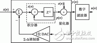
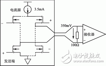
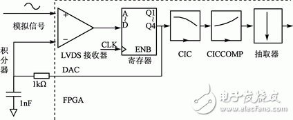
Digital systems have become more and more widely used in various fields of the real world. Most digital systems cannot directly process signals in the real world. ADC devices must be used to convert analog signals into digital signals before they can be processed. FPGA and DSP processors are the two mainstream technologies for digital signal processing. As technology advances and advances, some FPGA devices integrate analog circuits and mixed-signal processing modules, such as integrated temperature-monitoring diodes. Actel's hybrid FPGA family has integrated ADC, DAC, PGA (Programmable Gain Amplifier), voltage reference reference, and RC (Resistance Capacitance) oscillator. Xilinx's V5 series FPGAs integrate voltage and temperature monitoring ADCs, allowing users to read voltage and temperature values ​​directly from the JTAG download debug interface. However, these units have a fixed physical location and limited flexibility, and are limited to specific applications. The FPGA is implemented by the LVDS receiver of the FPGA. The logic circuit is completely implemented inside the FPGA. It can be reconfigured, has good scalability, and requires fewer peripheral devices, so that the FPGA can directly perform mixed signal processing. The core of the ΣΔ ADC is the ΣΔ modulator and digital filter. The principle of ΣΔ modulation was proposed more than half a century ago, but it was widely used in ADC design in the 1990s. The model of the ΣΔ ADC [1] is shown in Figure 1. Figure 1 ΣΔ ADC model As can be seen from the figure, the ADC of the ΣΔ architecture is mainly composed of an analog ΣΔ modulator in the left block and a digital filter on the right. The ΣΔ modulator consists of an integrator, an ADC, and a DAC that forms the feedback loop. The integrator is represented by discrete time to facilitate the Z-transform analysis. e(n) is the quantization noise of the AD quantizer. Assuming that the quantization noise is additive noise, the DAC in the feedback loop is ideal and its transfer function is a fixed gain. Using a linear system analysis method, let e(n) = 0, and consider the difference equation of the integrator: The system function that yields the integrator is: Examine the difference equation of the entire ΣΔ modulator: The system transfer function of the ΣΔ modulator to the signal is derived from equations (1) and (2): Let x(n)=0, the difference equation of the whole modulator to noise is: Therefore its noise transfer function is: From equations (5) and (6), the output of the entire ΣΔ modulator can be obtained as: It can be seen from equation (7) that in the Z-transform domain, the modulator only delays the signal and performs differential processing on the noise. Because the differentiator has a high-pass filter characteristic, the noise is high-pass filtered, and the time domain output of the modulator is: LVDS is a low-voltage, low-power, high-speed serial differential data transmission standard that is widely used in high-speed data interconnection and data communication. Mainstream FPGA devices integrate high-speed LVDS transceivers. The LVDS transceiver transmission block diagram is shown in Figure 2. Figure 2 LVDS transceiver block diagram In Figure 2, the four switching transistors at the LVDS transmitter cross control the flow of the 3.5 mA current source at the receiving end. The current establishes a voltage difference of approximately 350 mV across the 100 Ω resistor, and the receiver determines whether it is a logic "1" or a logic "0" by comparing the polarity of the voltage. The LVDS driver is current mode, is insensitive to power supply fluctuations, and consumes very little power. The power consumption of one LVDS transmission is 35 mA & TImes; 350 mV = 1.2 mW. Due to the differential transmission method, LVDS transceiver can eliminate common mode interference and improve system electromagnetic compatibility performance [2]. With the FPGA-integrated LVDS receiver, with a small number of peripherals, the ADC can be implemented inside the FPGA. Referring to the ADC principle of the ΣΔ architecture in Part 2, the block diagram of implementing the ADC inside the FPGA is shown in Figure 3. Figure 3 FPGA internal implementation of the ADC block diagram In Figure 3, the inside of the dashed box indicates implementation within the FPGA. Only one 1 kΩ resistor and one 1 nF capacitor are required as an analog integrator. The input signal and the integrator output value are compared in the LVDS receiver. The comparison result is quantized into a data bit stream, which is output to the CIC through the register. The (Cascaded Integrated Comb) filter [3] and its subsequent digital filtering module are simultaneously output to an external integrator through an FPGA pin as a 1-bit DAC. In the digital filtering module, the CIC filter accumulates the quantized bit stream and restores it to an 18-bit quantized value, while reducing the data rate by extracting a large multiple; CICCOMP is a 15th-order FIR filter [4] for compensation CIC filter amplitude response. The decimator is a 31-step FIR low-pass filter that reduces the data rate and further filters out-of-band noise. Dc Contactor,Special Contactor For Soft Starter,Latch Type Contactor,High Voltage Contactor NanJing QUANNING electric Co.,Ltd , https://www.quanningtrading.com

The remaining noise is filtered out by subsequent digital filters. 
