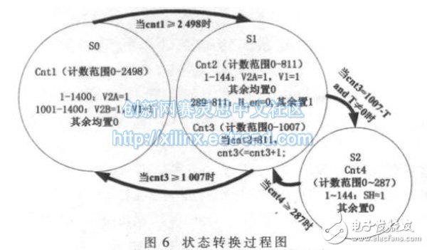
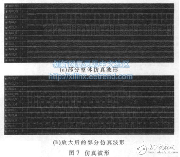
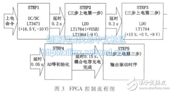
Abstract: For the driving requirements of the area array CCD KAI-1020 in the high frame rate mode, the FPGA is used as the control unit and timing generator to complete the hardware and software design of the CCD high frame rate mode. The simulation verifies the driving timing. Correctness, completed the debugging and testing of the hardware circuit. Imaging experiments show that the design satisfies the various drive control functions of the CCD KAI-1020 in dual-port output mode with an image resolution of 1 000 & TImes; 1 000 and a frame rate of 48 f/s. Charge Coupled Device (CCD) has been widely used in various imaging instruments since it was invented by Bell Labs in the 1970s due to its high resolution and small measurement error. The CCD is divided into two types, line array and area array, according to the imaging dimension. Linear array CCDs are only one-dimensional and need to be swept to form two-dimensional images. They are mainly used in spectrum analysis and image scanning. Surface array CCDs are widely used in digital because they can form two-dimensional images. Cameras, cameras and industrial robots [1]. The area array CCD is divided into three types: full frame transfer, frame transfer, and interline transfer according to the charge readout mode. Among them, the interline transfer CCD has been used as a high frame rate because it does not require a mechanical shutter and has the fastest readout speed. The first choice for CCD cameras. There are four main methods for driving the timing of CCD: direct digital circuit (IC) driving method, single-chip driving method, EPROM driving method, programmable logic device method, etc. [2]. In recent years, with the rapid development of programmable devices, FPGAs are very suitable for generating the driving timing of CCDs due to their high-speed parallel processing and extremely strong programming flexibility. In addition, they can well avoid the disadvantages of other driving methods. Therefore, it has become the first choice for CCD drive circuits. In this paper, for high-frame-rate high-resolution CCD camera applications with strict power consumption requirements, FPGA is selected as the driving control of high-speed interline transfer CCD, which can reduce the system volume and reduce the system power consumption. KAI -1020 is an inter-row transfer type area CCD produced by Kodak Company of the United States. The total number of pixels is 1 028 (H) & TImes; 1 008 (V), of which the effective pixels 1 000 (H) & TImes; 1 000 (V) , cell size 7.4 μm (V) & TImes; 7.4 μm (H), effective imaging area 10.5 mm [2-3]. KAI -1020 has progressive readout and interleaved readout (only 500 rows of CCD 1 000 rows of active imaging units are read). There are two ways, the maximum pixel readout rate is 40 MHz, and single or dual channel readout can be selected. . With progressive scan, dual channel readout, image resolution is 1 000 (H) × 1 000 (V), frame rate up to 48 frames / sec, this paper is designed to complete this mode of operation. To ensure the signal quality of the KAI-1020 in high frame rate mode of operation, a correlated double sampling circuit is integrated internally. After the imaging area is exposed, the optical signal is converted into a charge packet. Under the control of the driving signal, the charge packet is transferred to the adjacent storage area, and the charge signal is sequentially transferred, read, and sent to the internal integrated CDS circuit for sampling and output. . The KAI-1020 requires a complex drive signal for operation. It requires six kinds of bias voltages, and the voltage loading sequence also has certain requirements. The drive circuit is divided into three modules: voltage generation, FPGA control, and timing driver. The voltage generation module is used to generate various bias voltages required for FPGA and CCD operation; the FPGA control module is divided into a voltage control module and a timing generation module, which are respectively used to control the CCD voltage power-on sequence and the CCD drive timing generation; the timing driver is used to Match the FPGA port voltage to the CCD drive signal voltage. The driver hardware structure is shown in Figure 1. 2.1 Voltage Generation Module KAI -1020 requires three steps to power up due to internal structure requirements. The FPGA is used as the control unit. The operating voltages of +3.3 V, +2.5 V, and +1.2 V need to be loaded with the system. The camera bus voltage is +12 V. To ensure the normal operation of the CCD, reduce the power consumption of the system, and reduce the influence of voltage ripple and circuit noise during high-speed operation of the CCD. The voltage generation module uses DC/DC conversion with large differential pressure, and then small differential pressure. Linear regulator, a scheme that controls the power-up sequence by the FPGA. The power module voltage conversion process is shown in Figure 2. 2.2 FPGA Control Module For the miniaturization of the camera, the FPGA uses the XC3S400AN from the Xilinx Spartan-3AN series. The XC3S400AN is rich in resources, with 400,000 gates and up to 311 user I/Os. It integrates 4 Mbit Flash as a program storage area. It does not require an external configuration chip, making it ideal for space-sensitive and security-critical applications. After the camera is powered up, the FPGA completes the configuration and enters the working state. After receiving the power-on command, it controls the voltage loading by controlling the enabler of the voltage regulator to complete the CCD three-step power-on. The FPGA control flow is shown in Figure 3. After the -9 V voltage is applied, V1MID and V1MID (-1.2 V) are formed by conducting two diodes connected in series to ground. 2.3 timing drive module TI's SN74LV8T245 is an 8-bit conversion voltage adjustable, output tri-state, dual-supply bus transceiver with an internal AB split. The DIR control data flows from A to B or B to A. It can be configured from 1.65 V to 5.5 V. Configure DIR to 1, data flow to A to B, A to +3.3 V, interface to FPGA drive signal, B to +5 V, interface to CCD drive capacitor, FPGA and CCD drive voltage match. 3.1 Timing Analysis Among the KAI-1020 driving signals, the horizontal transfer signal and the CDS signal have the highest frequency of 40 MHz, and the duty ratios are 50% and 33.33%, respectively. There is a certain phase relationship between these signals, and the signals are transmitted through higher frequencies. Frequency implementation. The camera's operating clock is 30 MHz. After 8 times of the FPGA's DCM, the signal is divided by six and shifted to obtain 40 MHz signals of different phases. For low-frequency signals such as vertical transfer signals and electronic shutters, this is achieved by dividing the 40 MHz signal count. The implementation process is shown in Figure 5. 3.2 Logic design The driving timing is realized by the state machine, the frame transition is represented by the state s0, the vertical transition and the horizontal transition are represented by s1, and the delay requirement is completed by the counter counting, and the state transition process is as shown in FIG. 6. When the vertical transfer signal changes, the horizontal transfer signals H1, H2 need to maintain a high level and a low level, respectively. In the state s1, the signal H_en is set, and the H1 signal is obtained by ORing the H_en and the 40 MHz signal, and the H_en and the 40 MHz signal are OR'ed and then inverted to obtain the H2 signal. The electronic shutter signal SH needs to be loaded after a row of charge signals is read. Before the rising edges of the V1 and V2A signals, H1 and H2 need to change during this period. When the counter cnt3 counts the number of lines T required for exposure, the state machine jumps to the state s2, and after completing the SH signal delay, it jumps back to s1 to realize the electronic shutter 1-107 level adjustable. 3.3 Logic Simulation Through the timing analysis, the program is designed in VHDL language, the source code is written in Xilinx's integrated development environment ISE 10.1, and the simulation is performed. The simulation waveform is shown in Figure 7. Figure 7(a) shows a part of the overall simulation waveform. After V2B, V2A, and V1 are completed in the frame transfer phase, V2B is held low, and V2A and V1 are repeated. Figure 7(b) shows the horizontal transfer signal and the correlated double-sampled signal. Part of the simulation waveform, H1, H2 inversion, R, SA, SB, T phase relationship and timing requirements, when V2A, V1 change, H1 is high, H2 is low. After the simulation is passed, the VHDL source code is synthesized and implemented, and a programmable file is generated. After the file is downloaded to the FPGA, the CCD is controlled to generate an image signal, and the back-end processing circuit converts the analog image signal into a digital signal, and The two output image signals are spliced ​​to form a line image, and the image signal is sent to the data receiving end through the high-speed serial LVDS signal, the LVDS signal is decoded, and the image is formed on the host computer through the acquisition card. After actual imaging test, the CCD is driven by software and hardware, the frame rate is up to 48 frames per second, the image resolution is 1 000 (H) × 1 000 (V), and the exposure time can be 1 through the electronic shutter. 1007 level adjustment for flexible control of image brightness. Using FPGA as the control unit and timing generator of CCD KAI-1020, it is very convenient to generate various control and drive signals, complete CCD power-on sequence control and complex drive timing generation, and its powerful programmable and parallel processing capability is also very Conducive to system expansion and upgrade.
Bitmain Miner:Bitmain Antminer L7 (9.5Gh),Bitmain Antminer L7 (9.16Gh),Bitmain Antminer L7 (9.05Gh),Bitmain Antminer L3+ (504Mh),Bitmain Antminer L3+ (600Mh),Bitmain Antminer L3++ (580Mh),Bitmain Antminer L3++ (596Mh)
Bitmain is the world's leading digital currency mining machine manufacturer. Its brand ANTMINER has maintained a long-term technological and market dominance in the industry, with customers covering more than 100 countries and regions. The company has subsidiaries in China, the United States, Singapore, Malaysia, Kazakhstan and other places.
Bitmain has a unique computing power efficiency ratio technology to provide the global blockchain network with outstanding computing power infrastructure and solutions. Since its establishment in 2013, ANTMINER BTC mining machine single computing power has increased by three orders of magnitude, while computing power efficiency ratio has decreased by two orders of magnitude. Bitmain's vision is to make the digital world a better place for mankind.
Bitmain Miner,antminer L3 Miner,Asic L3 Antminer,Bitmain Antminer L7,ltc miner Shenzhen YLHM Technology Co., Ltd. , https://www.hkcryptominer.com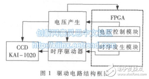
As a high-precision image sensor, CCD requires high power supply voltage stability and circuit noise level. The DC/DC power supply is highly efficient, but the ripple is large. The LDO power supply has good stability, but when the voltage difference is large, the heat is also large, which increases the system power consumption and circuit noise [4]. 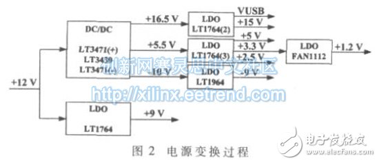
XC3S400AN Each BANK can be configured with a pin voltage of LVTTL or LVCOMS, but the CCD drive timing voltage is 0 to 5 V, so a level shifting chip needs to be added between the FPGA and the CCD.
The KAI-1020 operates in progressive scan and dual channel read mode. The main drive signals are V2B, V2A, V1, H1, H2, SH, R, SA, SB, and T. V2B is the frame transfer signal. At the falling edge, the CCD transfers the charge packets in the photosensitive cell to the memory cell; V2A and V1 are vertical transfer signals, which are responsible for transferring the charge packets of each row in the memory cell to the read register; H1 H2 is a horizontal transfer signal, which is responsible for reading each pixel in each line from the register; SH is an electronic shutter signal, a high pulse of SH can clear the charge accumulated by the previous exposure of the CCD, and the accumulation time of the charge becomes In order to control the exposure time from the falling edge of SH to the falling edge of V2B; R, SA, SB, T are the control timings of the correlated double sampling, R and T are in phase, and there is a certain phase difference with SA and SB. The timing relationship is shown in Figure 4. 

When the KAI-1020 is operating in the dual port read mode, the data on the left and right sides are read out in two ways. In the read register, there are 8 empty pixels in each of the left and right channels, and the horizontal transfer timing needs to be repeated 522 times to read one line of image data from the left and right. In order to ensure that the charge of the read line does not affect the next line of charge, the general horizontal transfer sequence is repeated at least 523 times, and the vertical transfer timing needs to be repeated 1 008 times, and the 1 008 lines of data are sequentially transferred from the storage area to the read register. 