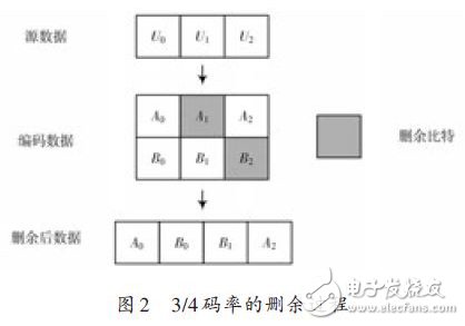
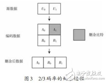
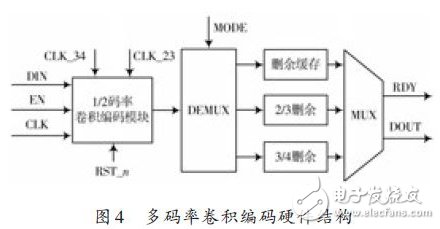
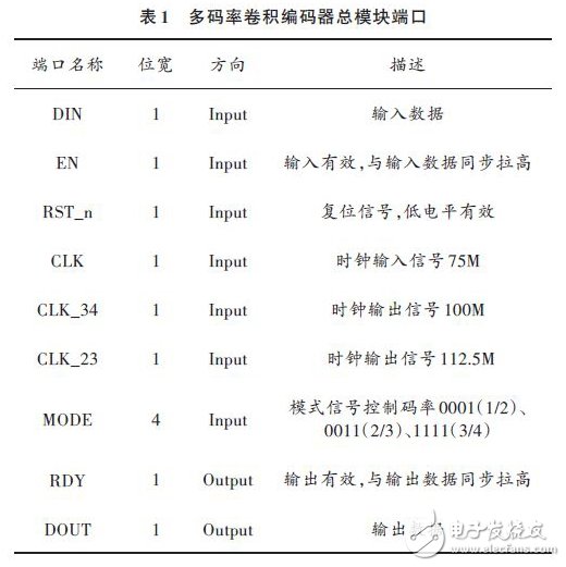
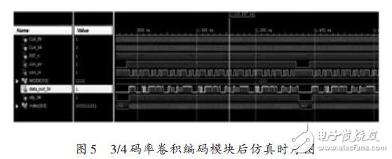
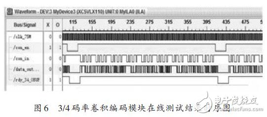
Abstract: In the L-band digital aeronautical communication system (L-DACS1), different types of data are transmitted at different rates. In order to reduce the noise and distortion of the channel and the influence of Doppler shift, multi-rate with good error control capability is adopted. Convolutional coding for channel error correction. The FPGA implementation and verification is completed by using Verilog HDL hardware description language. The test results show that the multi-rate convolutional encoder can adjust the code rate in real time, and perform error control efficiently and stably to meet the L-DACS1 high speed. The transmission remains stable and is used in actual projects. In order to address the high communication speed requirements and high bandwidth requirements brought about by the growth of ground-to-air data transmission services, the International Civil Aviation Organization (ICAO) requires civil aviation communications to transition from aeronautical-telecom-specific networks to a new generation of aviation networks. Therefore, EUROCONTROL in Europe proposed The Future Aeronautical Communication System (FAC), the L-band digital aeronautical communication system types 1 and 2 (L-DACS1 and L-DACS2), uses the L-band (960~1 164 MHz) to construct a new ground-to-air wireless data link. Improve data transmission speed and replace the previous narrowband communication system. In L-DACS1, due to the noise and distortion of the channel and the influence of Doppler shift, the transmitted information causes distortion and signal decision errors, and different types of data need to be transmitted at different rates, so multi-rate is required. Channel coding to reduce the bit error rate. Convolutional coding is a widely used channel coding technique, which has the ability to overcome burst errors, which can reduce the bit error rate of the channel and bring high coding gain. Therefore, multi-rate convolutional coding is an important part of the current L-DACS1. The convolutional code is usually represented by (n, k, N), where k is the number of data bits input to the encoder; n is the number of data bits output by the encoder; N is the length of the encoding constraint, and R = kn is the code of the convolutional code Rate. The subject of the (2,1,7) structure in the L-DACS1 protocol: convolutional coding, whose generator polynomial is [177,133], using three code rates of R=1/2, 2/3, 3/ 4. The convolutional encoder structure of the code rate R=1/2 used in L-DACS1 is shown in Fig. 1. In Fig. 1, D1D2D3D4D5D6 represents the state index of the encoder; U represents the input data bit; X(1)X(2 ) indicates the output data bits. In L-DACS1 baseband signal processing, in order to achieve higher rate and multiple different transmission rates, it is necessary to use puncturing operation based on 1/2 code rate convolutional coding to realize multi-rate convolutional coding. The puncturing process of 3/4 code rate is shown in Figure 2, and the 2/3 rate puncturing process is shown in Figure 3. In Fig. 2, the 3/4 code rate puncturing process is to input 3 b data, encode 6 b data, delete the fixed position 2 b, and finally generate a convolutional code with a code rate of 3/4 [8]. In Figure 3, the 2/3 code rate puncturing process is 2 b data per input, encoded as 4 b data, and 1 b is deleted at a fixed position, resulting in a convolutional code with a code rate of 2/3. The multi-rate convolutional coding module controls the transmission code rate of the data according to the mode signal (MODE) output by the main control unit, and determines whether the data is to enter the puncturing process and which puncturing processing unit to enter. Figure 4 shows the hardware implementation of the multi-rate convolutional code in L-DACS1. Table 1 shows the multi-rate convolutional encoder module port description. Figure 4 shows the operation of the multirate convolutional encoder as follows: The data is encoded by a CLK clock and input into a 1/2 code rate convolutional code module in the form of a serial bit stream, which is encoded. The module works in a synchronous manner. Each input 1 b will output 2-bit encoded data in parallel. According to the MODE control signal, it is determined which puncturing operation is performed after the 1/2 code rate convolution data to achieve 3/4 or 2/. 3 code rate. If 1/2 code rate encoding is used, since the implementation algorithm of the subsequent module requires data serial input, it is necessary to perform parallel/serial conversion, and the clock is increased to 2 & TImes; CLK_. To this end, a 2-bit merge string needs to be added. The output buffer unit is a puncturing buffer unit. If 2/3 and 3/4 code rate encoding is used, after processing by the 1/2 code rate convolutional coding module, the data is put into the corresponding puncturing buffer according to the MODE signal. The puncturing operation is to achieve the desired code rate. The output clocks CLK_23 and CLK_34 are 1.33 & TImes; CLK and 1.5 & TImes; CLK, respectively. The multi-rate convolutional encoder is simulated by Verilog HDL hardware description language [9]. The engineering files are synthesized, wired and simulated. The 3/4 code rate convolutional coding is taken as an example for analysis. The simulation results are shown in Fig. 5. Shown. In Figure 5, MODE is the mode control signal, and different puncturing modes can be selected according to the signal. Con_in is the input data of the module, and each time 144 b data is input continuously, the 1/2 code rate convolutional coding is performed first, and the data is It becomes 288 b, since the mode signal MODE is 1111, the puncturing operation of 3/4 code rate is performed, and serial data of 192 b is obtained, and the convolutional coded data of 3/4 code rate is output from the data_out_34 port by using the CLK_34 clock. . The project file passed through the simulation is added to the observation signal sampling clock, the trigger signal and the signal to be observed using ChipScope, and then re-synthesized, place-and-route to generate a bit file, downloaded to Xilinx's Virtex-5 series XC5VLX110-F1153 chip, and then used ChipScope. Online test, using the master clock 75 MHz, the test results are shown in Figure 6. In Figure 6, con_en represents the input enable signal, con_in represents the data before encoding, data_out represents the data after 3/4 rate encoding, and rdy_34 represents the signal with valid output data, the input clock frequency is 75 MHz, and the sampling clock frequency is 150. MHz. By comparing the simulation results of FIG. 5 with the online test results of FIG. 6, the correctness of the design under the high speed clock can be verified. This paper mainly describes the working principle of multi-rate convolutional encoder in L-DACS1, and realizes multi-rate convolutional encoder which can work normally under high-speed multi-rate condition by FPGA design. At the same time, it is designed with VerilogHDL hardware description language. The simulation verification was carried out. Finally, using the main clock frequency of 75 MHz, the hardware debugging, simulation and online test were performed under the Xilinx Virtex-5 series XC5VLX110-F1153 chip. The results showed that the expected design requirements were met. And used in actual projects.
Bitcoin mining equipment is mainly highly specialized ASIC mill , The maximum computing power of a single miner is 110T/s( Ant S19Pro mill ), The scale of computing power of the whole network is 120EH/s above . Ethereum's mining equipment is mainly graphics card mining machine , Professional ASIC Mining machines are very few , On the one hand, it is because of the of Ethereum mining algorithm [ resist ASIC sex " Improved R & D efficiency ASIC The threshold of the miner , So how much do you know about the mainstream Ethereum mining machine ?
Ethereum mining algorithm has higher requirements for memory , The purpose of this design limits ASIC The use of chips in Ethereum mining . From the results , Most Ethereum mining machines are graphics card machines , This reflects the application of Ethereum mining algorithm ASIC Success on . From the absolute value of computational power scale , The computing power of Ethereum is about 200TH/s, The computing power of bitcoin is about 120EH/s, The latter is close to the former 60 ten thousandfold .
ASIC Mining machines have high computing power , Large power consumption , Like the latest ant S19Pro mill , Rated power consumption is 3250W, Need to consume... Every day 78 Degree electricity , According to the current currency price and 0.23 The electricity price in wet season is RMB , The proportion of electricity charge is 30.68%. Other older bitcoins ASIC mill , Like ants T17 series , The proportion of electricity charges generally exceeds 50%. by comparison , The power consumption of the graphics card miner is low , The proportion of electricity is also low . such as 5600XT8 Graphics card miner of card .
Ant S19-95T It adopts aluminum alloy profile electromechanical integrated design , Parallel four fan structure . According to the measured data , In line with and better than the official data .S19 The series is provided by TSMC 7nm chip , A new generation of customized chips with perfect whole machine architecture and high conversion rate APW12 Power Supply , Reduce power loss during conversion , Use more energy-saving , Greatly shorten the return cycle of the miner . In addition, the newly upgraded mining machine operation interface is also more humanized , Real time computing power . The average computing power and the operation of each chip are clear at a glance .
Shenma mining machine M30S-86T/88T/90T, Bit micro 2020 Launched in 2013 M30S Series of new mining machines , Announced that it would M30S The series is expanded to three 3X product . stay 3X In the new standard , Bit micro promises a one-year warranty for its series of products . This series of mining machines are provided by Samsung 8nm chip , Among them, god horse M30S series , The power consumption is 38J/T, Provide higher computing power , Lower power consumption and high stability.
Ethereum Mining Machine:Jasminer X4,Bitmain Antminer E9 (2.4Gh),iPollo V1,Jasminer X4-1U,iPollo V1 Classic, Ethereum Mining Machine,ETHW Miner,innosilicon a10 pro,E9 Antminer,Innosilicon A11 Shenzhen YLHM Technology Co., Ltd. , https://www.ylhm-tech.com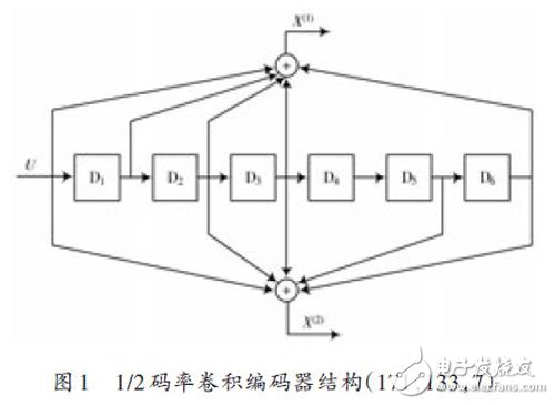
Jasminer X4-C 1U,iPollo V1 Mini SE Plus