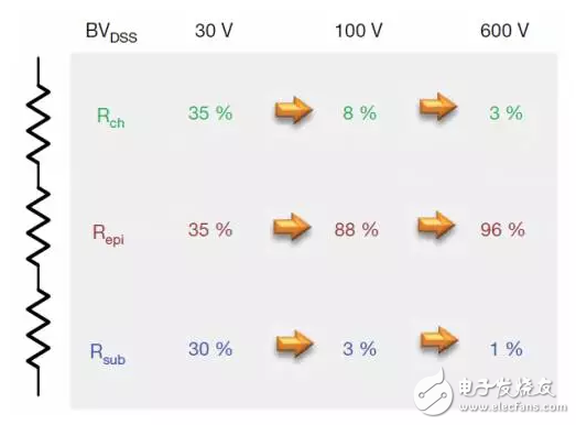
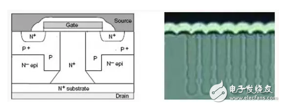
Power MOSFETs based on super junction technology have become the industry standard in the field of high voltage switching converters. They offer lower RDS(on) with less gate and output charge, which helps maintain higher efficiency at any given frequency. Prior to the advent of super-junction MOSFETs, the main design platform for high-voltage devices was based on planar technology. At this time, an anxious netizen should ask, what kind of technology is super-junction, different from plane technology, and where is its advantage? Dear friends, you will understand after reading this article! Figure 1 shows a simple structure of a conventional planar high voltage MOSFET. Planar MOSFETs typically have high unit chip area drain-source on-resistance with relatively high drain-source resistance. Lower RDS(on) values ​​can be achieved using high cell densities and large die sizes. However, large cell density and die size are accompanied by high gate and output charge, which increases switching losses and cost. There is also a limit to how low the total silicon resistance can be. The total RDS(on) of the device can be expressed as the sum of the three components of channel, epi, and substrate: RDS(on) = Rch + Repi + Rsub Figure 1: Traditional planar MOSFET structure Figure 2 shows the components that make up RDS(on) in the case of a planar MOSFET. For low voltage MOSFETs, the three components are similar. However, as the rated voltage increases, the epitaxial layer needs to be thicker and lighter doped to block the high voltage. For every doubling of the rated voltage, the area required to maintain the same RDS(on) is increased by more than five times. For MOSFETs rated at 600V, more than 95% of the resistance comes from the epitaxial layer. Obviously, in order to significantly reduce the value of RDS(on), it is necessary to find a method of heavily doping the drift region and greatly reduce the epi resistance. Figure 2: Resistive components of planar MOSFETs Typically, high voltage power MOSFETs have a planar structure in which a thick, low-doped N- epitaxial layer, the epi layer, is used to ensure sufficient breakdown voltage, low doped N-epi layer size The thicker, the higher the withstand voltage rating, but the on-resistance also increases sharply. The on-resistance increases with voltage from 2.4 to 2.6 power, thus reducing the current rating. In order to obtain a certain on-resistance value, it is necessary to increase the area of ​​the silicon wafer, and the cost increases. If a similar minority carrier conduction is introduced similar to an IGBT, the turn-on voltage drop can be reduced, but the introduction of minority carriers reduces the switching frequency of the operation and produces a current tailing that is turned off, thereby increasing switching losses. The epitaxial layer of the high-voltage power MOSFET plays a dominant role in the total on-resistance. To ensure that the high-voltage power MOSFET has sufficient breakdown voltage and reduce the on-resistance, the most intuitive method is: when the device is turned off, Let the low-doped epitaxial layer ensure the required withstand voltage level, and at the same time, when the device is turned on, a highly doped N+ region is formed as the current path when the power MOSFET is turned on, that is, the reverse blocking voltage and the conduction The above requirements can be achieved by separating the on-resistance functions and designing them in different areas. A high-voltage power MOSFET based on the super-junction SuperJuncTIon's built-in lateral electric field is a new type of device designed with this idea in mind. A schematic diagram of the cross-sectional structure of a high voltage MOSFET with a built-in transverse electric field and a high blocking voltage and low on-resistance is shown in FIG. Infineon first produced this structure and designed a trademark CoolMOS for this type of MOSFET. This structure is academically called super-junction power MOSFET. Figure 3: SuperJuncTIon structure with built-in transverse electric field The vertical conductive N+ region is sandwiched between the P regions on both sides. When the MOS is turned off, two reverse biased PN junctions are formed: P and vertical conductive N+, P+ and epitaxial epi layer N-. The P region under the gate cannot form an inversion layer to generate a conductive channel, P and the vertical conductive N+ form a reverse bias of the PN junction, the PN junction depletion layer increases, and a lateral horizontal electric field is established; meanwhile, the P+ and the epitaxial layer The N-forming PN junction is also reverse biased, creating a wide depletion layer and establishing a vertical electric field. Since the doping concentration of the vertical conductive N+ region is higher than the doping concentration of the epitaxial region N-, and the horizontal horizontal electric field is generated on both sides of the vertical conductive N+ region, substantially the entire region of the vertically conductive N+ region becomes a depletion layer, that is, From N+ to N-, such a depletion layer has a very high longitudinal blocking voltage, and therefore, the withstand voltage of the device depends on the withstand voltage of the highly doped P+ region and the N-region of the low doped epitaxial layer. When the MOS is turned on, the electric field of the gate and the source inverts the P region under the gate, and the N region under the gate generates an N-type conductive channel, and at the same time, the electrons in the source region enter the vertical through the conductive channel. The N+ region neutralizes the positively charged holes in the N+ region, thereby restoring the depleted N+ type characteristics, so that the conductive channel is formed, the vertical N+ region has a high doping concentration, has a low resistivity, and thus has low on-resistance. . Comparing the power MOSFETs of planar structure and trench structure, it can be found that the super junction structure is actually a combination of both planar and trench structures, and is a trench with a low impedance current path in a planar structure. Therefore, it has a low-resistance characteristic of a high withstand voltage and a groove type structure of a planar structure. Compared with the planar structure, the high-voltage super junction structure with built-in transverse electric field can design a lower on-resistance and therefore have a larger rated current value and avalanche energy. Due to the need to open the N+ trench, its production process is more complicated. At present, N+ trenches are mainly produced by two methods: N+ trenches and direct trenches are obtained by epitaxial growth layer by layer. The former process is relatively easy to control, but the process has many procedures and high cost; the latter has low cost, but it is not easy to ensure the consistency of performance in the groove.
Docking station
Docking stations for laptops are meant to bridge the gap between portability and having a stationary place to work and play.With a docking station,you can get the best of both worlds with a system that allows your laptop to work for both purposes.Some of the most basic docking stations provide a power supply and ports for connecting to other devices.More advanced docking stations may inclade space for additional PC monitors,keyboards,and computer speakers.It can also have additional USB-C ports to connect to printers,add external hard drives,and connect microphones and audio.
Docking Station,Macbook Docking Station,Macbook Pro Docking Station,Usb C Docking Station Pogo Technology International Ltd , https://www.wisesir.net


