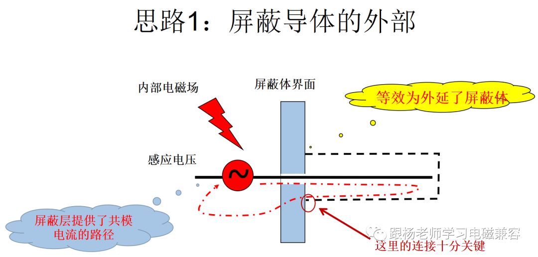
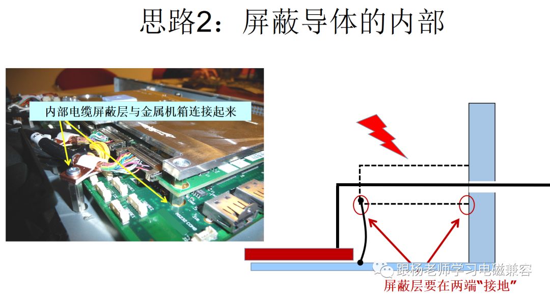
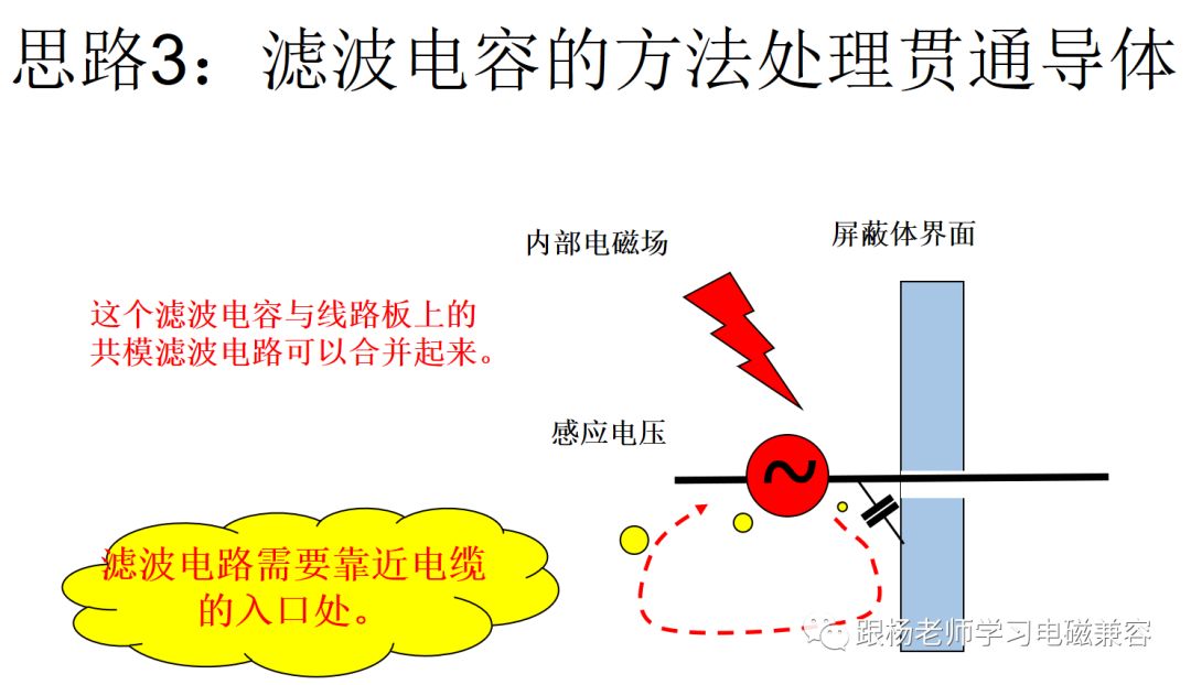
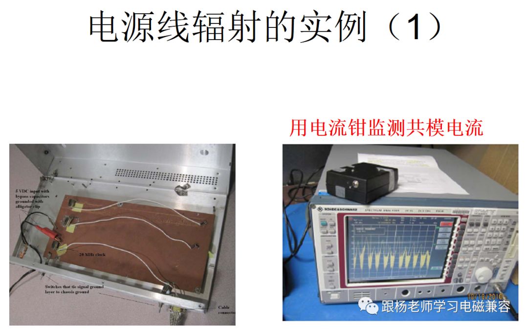
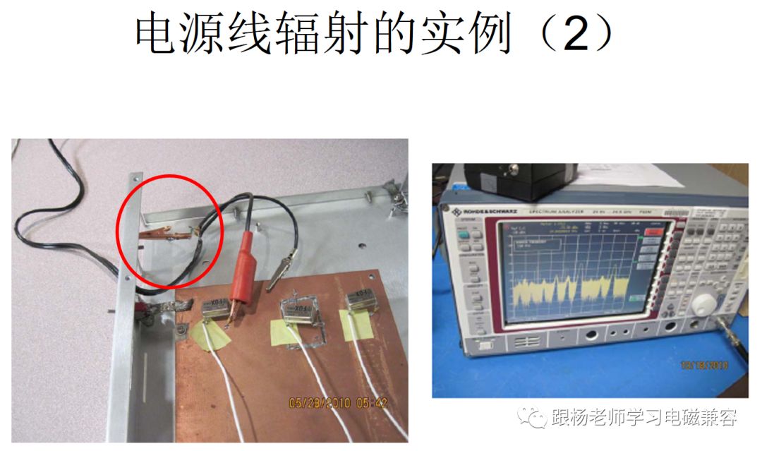
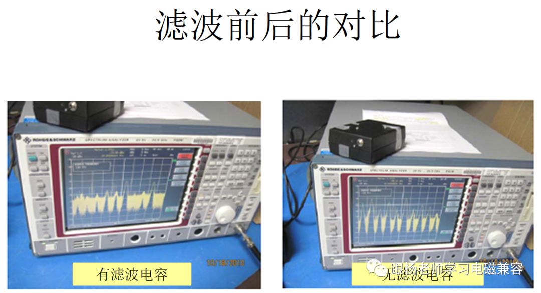
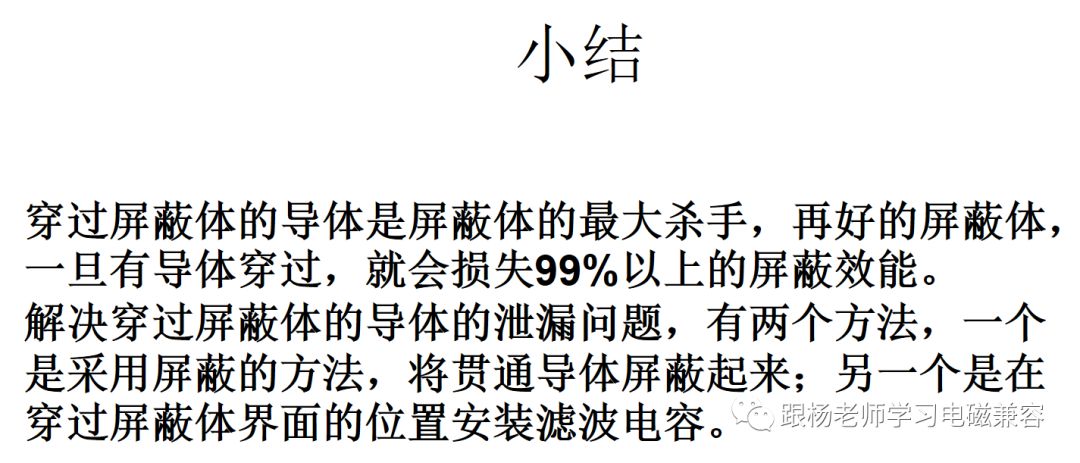
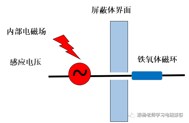
The various external cables on the device are the conductors that pass through the shield case. Designers think that the basic method to solve the problem of electromagnetic radiation of these cables is shielding. However, in reality, there are few cases where the desired effect is achieved through shielding. This is because there is no understanding of the nature of shielding to solve the cable radiation. The figure shows a case where a conductor passes through the shield interface. In order to prevent the internal electromagnetic field from leaking through this conductor, we shielded the conductor on the right side of the shield interface. It can be seen that, at this time, it can actually be seen as a part of the shielding interface being extended. In fact, there is no case where the through conductor passes through the shielding interface, and of course there is no electromagnetic leakage. We can also explain the effectiveness of shielding from the perspective of common-mode current paths. With additional shielding, the common-mode currents on the conductors can return to the source of disturbance through this additional shield. This path is obviously much smaller than the original path and therefore produces less electromagnetic radiation. Please pay attention to a detail, that is, no matter which kind of mechanism, you need a guarantee condition, this is the additional shield must be conductively connected with the original shield, otherwise, the mechanism does not become a complete shield, nor can it be a total The modulo current provides a return path. In fact, the overlap between the two shields is very important, ideally 360 degrees (one week) continuous overlap. The same effect can be achieved by shielding the conductor inside the device. The right figure shows the shielding of the inside of the through conductor. Due to the additional shielding, the voltage induced on the conductor by the internal electromagnetic field is weakened, so that electromagnetic leakage is also reduced. Here also need to pay attention to the "grounding" of the additional shield, that is, the conductive connection with the original shield. The additional shield should be grounded at both ends and the lap impedance should be kept as low as possible. The figure on the left is an example of an actual internal cable shield. Here, the shield is well crimped to ensure low impedance grounding. Shielding the through-conductors (cables) internally is often unsatisfactory. One of the reasons is that the cables are always connected to the circuit on the PCB. Even if we shield the cables, the PCB is still exposed. Therefore, no The induced voltage may be completely eliminated unless the PCB is shielded together. A very effective method is to install a high-frequency capacitor between the through-conductor and the shield interface at the position where the through-conductor passes through the shield interface. At this time, the electromagnetic leakage of the through-conductor will be greatly reduced. The principle of this method is shown in the figure. When we analyzed the electromagnetic leakage of the through-conductor, we analyzed the path of the common-mode current. The stray capacitance between the conductor and the shield interface is an important part of the common-mode current path. Now, we consciously provide a capacitor that changes the original common-mode current path. This newly added capacitance provides a path back to the disturbance source for the common mode current, so the common mode current will not be conducted along the conductor to the other side of the shielded interface, and it will not cause electromagnetic leakage. Specifically how much current will be shunted from this newly added capacitance depends on the ratio of the path impedance provided by the newly added capacitor to the original common-mode current path impedance. This is similar to the case of the current of two resistors when we calculate the resistance parallel circuit. The higher the original path impedance, the more pronounced the effect of the newly added capacitance. The impedance of the original common-mode current path is related to the length of the cable and the laying method. Sometimes, we put a ferrite ring on the cable, which actually acts to increase the impedance of the external loop. We have taken an example to deepen our understanding of the filter capacitor method mentioned above. The left figure is an experimental device. Install a clock circuit on a PCB. As we know before, the clock circuit is the most typical harassment source circuit. Therefore, we generally use this kind of circuit to do experiments. The PCB is placed in a metal shield box and powered by an external DC power supply. We use a current clamp to monitor the common-mode current on the power line. The right figure is a spectrum analyzer and current clamp used to monitor common-mode currents. Spectrum of the common-mode current displayed on the spectrum analyzer. It is a very useful method to indirectly predict the radiation of the cable by monitoring the common mode current on the cable. Designers should be familiar with it and be able to use it skillfully. Later, we will give a method for predicting radiation from common-mode currents. The left picture shows a case where a capacitor is connected between the power line and the metal case. The red circle in the figure shows the state of connecting the capacitor to the metal shell with alligator clips. The spectrum analyzer on the right shows the common mode current at this time. As can be seen, the amplitude of the common-mode current has been greatly reduced. This shows that part of the common-mode current is shunted by the capacitor and is not conducted to the external power line. In order to make it easy for us to compare the situation before and after the filtering, we have filtered and common mode current spectrum together without filtering. On the left there is a filter capacitor and on the right there is no filter capacitor. The difference between them is clear at a glance. Thinking questions: Due to the presence of a conductor that penetrates the shield, the radiation emission exceeds the limit. The designer put a ferrite ring on the conductor. Please predict how much this ferrite ring can reduce the radiation. Right Angle DIP Centronic Connector
Right Angle DIP Centronic Connector.
Current Rating:5A Right Angle DIP Centronic Connector ShenZhen Antenk Electronics Co,Ltd , https://www.atkconnectors.com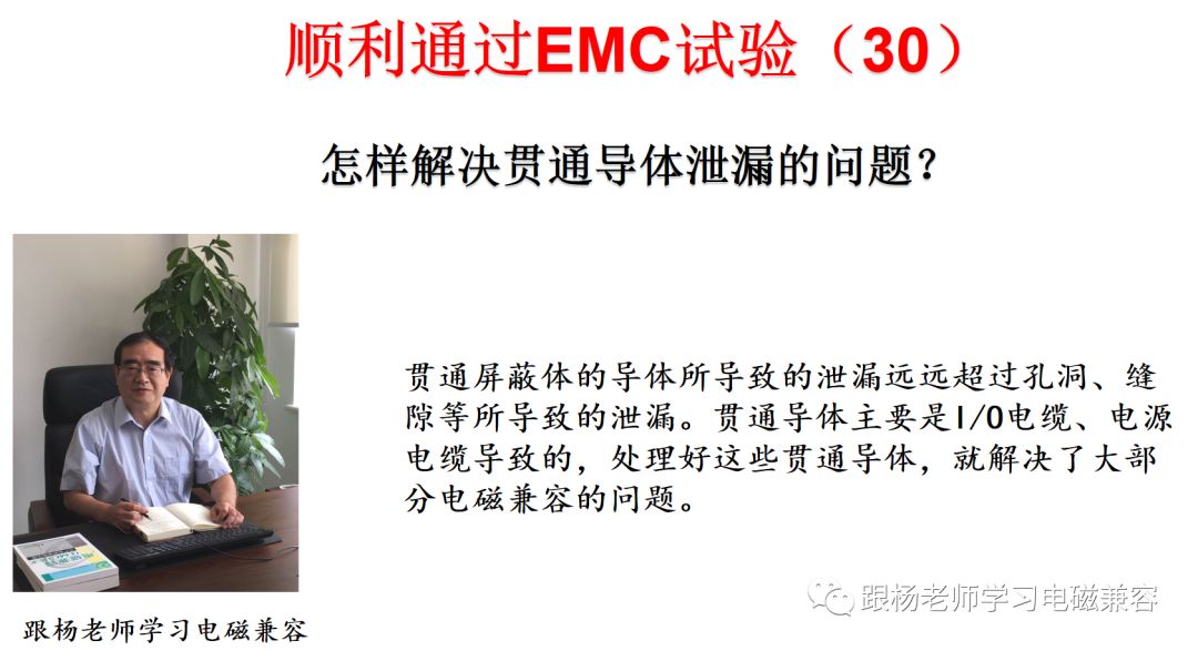
Dielectric Withstanding Voltage:1000V for one minute
Insulation Resistance:1000MΩ Min.(at 500V DC)
Contact Resistance:35mΩ Max.
Temperature:-55°C to +105°C