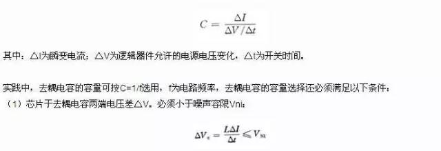
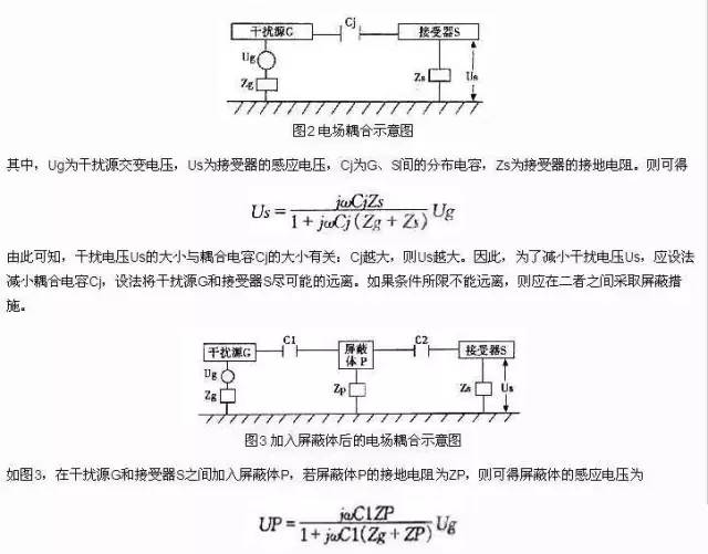
The main ways of electromagnetic interference are conducted interference, radiated interference, common impedance coupling and inductive coupling. The corresponding countermeasures should be adopted for the interference caused by these several ways: transmission filtering, radiation interference using shielding and grounding, etc., can greatly improve the product's ability to resist electromagnetic interference, and can also effectively reduce electromagnetic interference to the outside world. . This paper introduces EMC's design skills from four perspectives: filter design, grounding design, shielding design and PCB layout and routing skills. Decoupling Capacitor Capacity Selection In digital systems, the capacity of decoupling capacitors is usually estimated as follows: Second, EMC grounding design grounding is the most effective way to suppress the source of disturbance, which can solve 50% of EMC problems. The system ground is connected to the ground to suppress electromagnetic disturbances. The metal parts of the case are directly connected to the ground, and can also provide an electrostatic charge leakage path to prevent static electricity from accumulating. In the ground line design, the following points should be noted: (1) Correct selection of single-point grounding and multi-point grounding In the low-frequency circuit, the operating frequency of the signal is less than 1MHz, and its wiring and the inductance between the devices are less affected, and the grounding circuit The formed circulation has a great influence on the interference, so a single point grounding should be used. When the signal operating frequency is greater than 10MHz, the ground line impedance becomes very large. At this time, the ground line impedance should be reduced as much as possible. When the operating frequency is between 1 and 10 MHz, if a grounding is used, the grounding length should not exceed 1/20 of the wavelength. Otherwise, the multi-point grounding method should be used. (2) Separating the digital circuit from the analog circuit On the circuit board, there are both high-speed logic circuits and linear circuits. They should be separated as much as possible, and the ground wires of the two should not be mixed, and they are connected to the ground of the power supply. Try to increase the grounding area of ​​the linear circuit. (3) Try to thicken the grounding wire. If the grounding wire is very thin, the grounding potential changes with the change of the current, causing the timing signal level of the electronic device to be unstable and the anti-noise performance to deteriorate. Therefore, the ground wire should be as thick as possible so that it can pass the three allowable currents on the printed circuit board. If possible, the width of the ground wire should be greater than 3mm. (4) When the grounding wire is formed into a closed-loop circuit. When the grounding system of the printed circuit board consisting of only digital circuits is designed, the grounding wire can be made into a closed-loop circuit to significantly improve the anti-noise capability. The reason is that there are many integrated circuit components on the printed circuit board, especially when there are components with high power consumption, due to the limitation of the thickness of the grounding wire, a large potential difference will be generated on the ground junction, causing the noise resistance to decrease. If the ground structure is looped, the potential difference will be reduced to improve the noise immunity of the electronic device. Third, EMC shielding design shielding is to control the interference of an electric field or magnetic field in one area to another area by the principle of metal isolation. It includes two meanings: one is to surround the circuit, cable or the interference source of the whole system to prevent electromagnetic interference from spreading outward; the other is to surround the receiving circuit, equipment or system with a shield to prevent them from being electromagnetically disturbed by the outside. influences. Shielding can be divided into three different ways: electric field shielding, magnetic field shielding, and electromagnetic field shielding according to the mechanism. The electric field in an electric field shielding electronic device is usually an alternating electric field, so the electric field induction between the two systems can be considered as the coupling of the distributed capacitance Cj between the two systems, as shown in FIG. 1. Choosing a reasonable wire width Because the transient interference generated by the transient current on the printed line is mainly caused by the inductance component of the printed wire, the inductance of the printed wire should be minimized. The inductance of a printed conductor is proportional to its length and inversely proportional to its width, so that short and precise conductors are advantageous for suppressing interference. Signal lines for clock leads, row drivers, or bus drivers often carry large transient currents, and the printed conductors should be as short as possible. For the discrete component circuit, when the width of the printed conductor is about 1.5mm, the requirement can be fully satisfied; for the integrated circuit, the width of the printed conductor can be selected between 0.2 and 1.0mm. 2. Several aspects to be aware of when wiring with the correct routing strategy: (1) Keep the loop area to a minimum, reduce the impact of interference on the system, and improve the anti-jamming performance of the system. The parallel wires are placed tightly together, and a thick wire is used for connection. The signal line is close to the ground plane to reduce interference. Add high frequency filter capacitors between the power supply and ground. (2) Make the length of the wire as short as possible, reduce the area of ​​the printed board, and reduce the interference on the wire. (3) Adopting a complete ground plane design, using a multi-layer board design, laying the ground layer to facilitate interference with signal bleed. (4) Keep the electronic components away from planes that may discharge, such as chassis panels, handles, screws, etc., to keep the casing in good contact with the ground, providing a good venting channel for interference. Handling sensitive signals to reduce interference. (5) Try to use SMD components. (6) Ground the analog ground and the digital ground at the connection between the PCB and the outside world. (7) The high-speed logic circuit should be close to the edge of the connector, the low-speed logic circuit and memory should be placed away from the connector, and the medium-speed logic circuit should be placed between the high-speed logic circuit and the low-speed logic circuit. (8) Do not change the width of the printed circuit board on the circuit board. The corner should be rounded, not right angle or sharp angle. (9) The clock line and signal line should also be as close as possible to the ground line, and the trace should not be too long to reduce the loop area of ​​the loop. 3. Printed circuit board size and device layout Printed circuit board size should be moderate. When the size is too large, the printed lines are long, the impedance is increased, not only the anti-noise ability is lowered, but also the cost is high; if it is too small, the heat dissipation is not good, and at the same time, it is susceptible to interference from adjacent lines. In terms of device layout, as with other logic circuits, the related devices should be placed as close as possible to achieve better noise immunity. Clock generators, crystal oscillators, and CPU clock inputs are prone to noise and are close to each other. Devices that are prone to noise, small current circuits, high-current circuits, etc. should be kept away from the logic circuit as much as possible. If possible, a separate board should be used.
Automotive Connector Housing.
Automobile connector is a kind of component that electronic engineers often contact. Its function is very simple: in the circuit is blocked or isolated between the circuit, set up a bridge of communication, so that the current flow, so that the circuit to achieve the intended function. The form and structure of automobile connector are ever-changing. It is mainly composed of four basic structural components: contact parts, shell (depending on the type), insulator and accessories
Automotive Connector Housing ShenZhen Antenk Electronics Co,Ltd , https://www.antenksocket.com
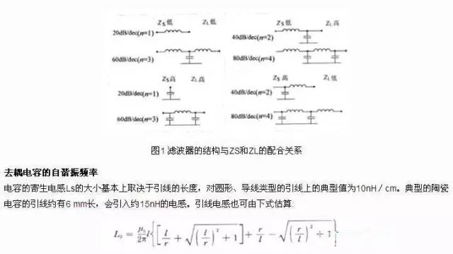
I. EMC Filter Design Techniques Filters in EMC design usually refer to low-pass filters composed of L and C. The choice of filter structure is determined by the "maximum mismatch principle". That is, in any filter, there is a high impedance across the capacitor and a low impedance across the inductor. Figure 1 shows the relationship between the structure of the filter and the ZS and ZL obtained by the principle of maximum mismatch. In each case, two structures and corresponding attenuation slopes are given (n indicates the total number of capacitive and inductive components in the filter). . 
Where: l and r are the length and radius of the lead, respectively. The parasitic inductance will generate series resonance with the capacitor, that is, self-resonance. At the self-resonant frequency fo, the decoupling capacitor exhibits the least impedance and the decoupling effect is best. However, for a noise component with a frequency f higher than f/o, the decoupling capacitor is inductive, and the impedance becomes larger as the frequency increases, so that the decoupling or bypassing effect is greatly reduced. In practice, the self-resonant frequency f0 of the decoupling capacitor should be selected according to the highest frequency fmax of the noise, and the best value is fo=fmax. 


Then the induced voltage on the receiver is:  From this, it can be seen that to reduce the induced voltage Us of the receiver, Zp should be as small as possible. Therefore, the shield must be selected from materials with good electrical conductivity and must have good grounding. Otherwise, because Cl>Cj, C2>Cj, if the grounding resistance of the shield is large, the interference caused by the addition of the shield will become larger. Magnetic field shielding magnetic field shielding refers to shielding of low frequency magnetic fields and high frequency magnetic fields. The shielding of the low frequency magnetic field uses a ferromagnetic material with high magnetic permeability. The high magnetic permeability of the ferromagnetic material is used to shunt the disturbing magnetic field, so that the magnetic flux passing through the air is greatly reduced, thereby reducing the influence on the interfered source and functioning as a magnetic field shield. Since it is a magnetic shunt, the higher the magnetic permeability U of the shielding material shielding material, the thicker the shield shielding cover, and the more magnetic flux that the magnetic shunt flows, the better the shielding effect. The shielding of the high-frequency magnetic field uses a good conductor of low resistivity as a shielding material for the shielding material. The external high-frequency magnetic field generates eddy currents in the shield, and the magnetic field formed by the eddy current suppresses and cancels the external magnetic field, thereby playing a shielding role. Unlike low-frequency magnetic shielding, due to the skin effect of high-frequency eddy currents, the size of the shielding body is not the key to the shielding effect, and the grounding of the shielding body and the shielding effect are also irrelevant. However, for a good metal conductor with high-frequency magnetic shielding, if there is good grounding, it has the effect of electric field shielding and magnetic field shielding. Therefore, the shield of the high-frequency magnetic shield should also be grounded. The electromagnetic field shielding electromagnetic field shielding uses the shielding body to shield the electric field and the magnetic field at the same time, and is generally used for shielding the high frequency electromagnetic field. As can be seen from the above, for a high-frequency interference voltage, a good conductor is selected to form a shield, and a good grounding is provided to shield the electric field and the magnetic field at the same time. However, it must be noted that the eddy current shielded by the high-frequency magnetic field not only adversely affects the external interference, but also may adversely affect the inside of the device protected by the shield, thereby generating new interference.
Fourth, PCB layout layout strategy