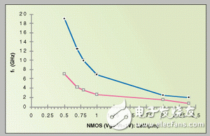
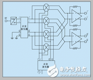
In recent years, research on the possibility of applying CMOS processes to radio frequency (RF) technology has increased dramatically. Deep submicron technology allows CMOS circuits to operate at frequencies above 1 GHz, which undoubtedly drives the development of integrated CMOS RF circuits. Several research groups have developed high performance downconverters, low phase noise voltage controlled oscillators (VCOs) and dual modulus prescalers using standard CMOS processes. These studies show that fully integrated receiver and VCO circuits can be designed without the need for additional components or adjustments. In-depth research into low noise amplifiers, upstream converters, synthesizers, and power amplifiers will likely design fully integrated transceiver CMOS RF circuits for telecom applications. The rapid development of wireless communication and its application technology is largely due to the introduction of digital coding and digital signal processing technology in wireless communication. The development of digital technology is the result of the development of high-performance, low-cost CMOS technology, because CMOS technology makes it possible to integrate a large number of digital functions on a single die. Thus, the use of advanced modulation techniques, sophisticated demodulation algorithms, and high quality error detection and correction systems results in a high performance lossless digital communication channel. At present, the development of digital technology and the rapid growth of the wireless market have dramatically changed the analog transceiver front-end equipment. The front-end device is the interface between the antenna and the digital modem of the wireless transceiver. The front-end device must detect weak signals at frequencies up to 1 GHz to 2 GHz microvolts. At the same time, it is necessary to transmit a signal having a power of about 2 W at the same high frequency. Therefore, this requires high-performance analog circuits such as filters, amplifiers, and mixers that can convert frequency bands between antennas and A/D conversion and digital signal processing. Low cost and low power requirements make analog front-end equipment a bottleneck for future RF designs, and further improvements in integration will significantly reduce die size, cost and power consumption. In the past few years, many different techniques have been proposed to further enhance the integration of receivers, transmitters and synthesizers. While further increasing the level of integration, researchers are also trying to integrate RF circuits in a CMOS process. Although CMOS technology is mainly used in the integration of digital circuits, if CMOS technology can be applied in high-performance analog circuits, the performance will be greatly improved, and the advantages will be more obvious: a complete transceiver can be integrated on a single chip. The system, which integrates both analog front-end devices and digital demodulator on the same die. This requirement can only be achieved with CMOS or BiCMOS processes. The BiCMOS process can improve the performance of the analog design, but the cost is correspondingly increased, not only because of the increased cost per unit area, but also by the need to reserve more chip space for the digital circuit portion. As investments in CMOS processes far exceed bipolar devices, common CMOS processes will gradually eliminate BiCMOS devices from NMOS devices using deep sub-micron CMOS processes, and even eliminate performance differences between NMOS devices using the same BiCMOS process. The ft parameter of the NMOS device will gradually approach the ft of the NPN device. Although some RF design studies using CMOS technology have been carried out many years ago, it is only in recent years that people really pay attention to the possibility of implementing this technology. Currently, several research groups in the industry are working on this topic. Because bipolar devices are inherently superior to CMOS devices, some researchers believe that RF CMOS is only suitable for low performance systems with lower performance standards, such as ISM, or can be improved by CMOS processes such as etching under the inductor. To improve its performance. RF CMOS technology will likely fully integrate high-performance applications such as GSM, DECT and DCS1800 in a common deep sub-micron process. CMOS technology Submicron technology is now considered standard CMOS technology due to the increasing technical standards and the consideration of higher integration DSP circuits. The trend of this technology has even evolved into deep submicron technology, such as transistors with specifications of 0.1 micron or less. Transistors with Ft close to 100 GHz have recently appeared in deep sub-micron processes of 0.1 micron. However, parasitic capacitance in transistors, including gate-drain overlap capacitance and drain-bulk juncTIon capacitance, has slowed the development of deep sub-micron technology. Figure 1 compares the ft and fmax values ​​for different techniques, which clearly illustrates the above conclusions. Compared to ft, fmax is more important because fmax reflects the rate limit of the transistor in the actual configuration. As shown in the figure, although ft increases rapidly, the speed improvement is not large for the actual circuit design (fmax). Finally, it is clear in recent integrated CMOS RF circuits that not only CMOS technology itself is a limiting factor, but the same is true for packaging. Since the RF signal will ultimately originate from the chip, and since the RF antenna signal must enter the chip, any PCB or package pin parasitic capacitance connected to the ESD protection network will greatly affect or degrade the RF signal. Receiver topology A heterodyne or intermediate frequency receiver is the most commonly used receiver topology. In an intermediate frequency receiver, the desired signal will be downconverted to a relatively high intermediate frequency. The use of a high quality passive bandpass filter prevents the image signal from overlapping the desired signal at the IF frequency. Extremely high receiver performance can be achieved by utilizing an IF receiver topology, especially when multiple IF stages are employed.
The JUK universal Screw Terminal Block series has the typical features which are decisive for practical applications:
l The universal foot allows the terminal blocks to be easily snapped onto the NS35 or NS32 DIN Rail with G shape.
l Closed screw guide holes ensure screwdriver operation perfect.
l For terminal block with different wire cross-sectional areas, complete accessories are available, such as end plates, partition plates, etc.
l Potential distribution achieved by fixed bridges in the terminal center or insertion bridges in the clamping space.
l Same shape and pitch Grounding Terminal Blocks as the JUK universal series.
l Adopt ZB marker strip system,achieve unified identification.
Double Level Terminal Blocks,Fuse Hold Terminal Block,Weidmuller Sak Terminal Block,Fuse Terminal Block Wonke Electric CO.,Ltd. , https://www.wkdq-electric.com
