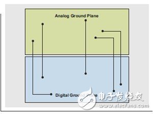
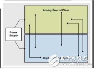
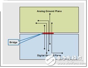
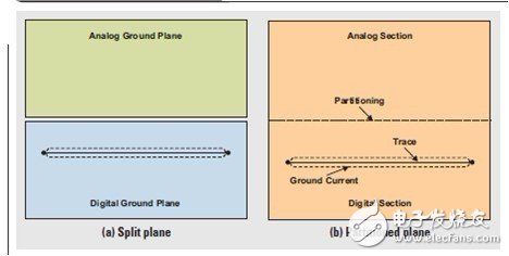
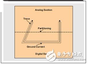
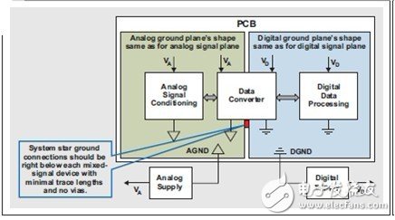
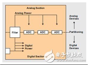
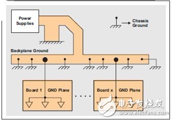
Author: Texas Instruments (TI) analog applications engineer Sanjay Pithadia And senior simulation application engineer Shridhar More This article is the second in a series of 2 articles. Part 1 (see Reference 1) explains some typical terminology and ground planes and introduces the partitioning method. Part 2 will discuss the pros and cons of splitting the ground plane. In addition, the article will explain the multi-converter and multi-board system grounding. If the ground plane is split and the line passes through the split line (as shown in Figure 1), where is the current return path? Assuming that the two layers are connected somewhere (through a single point), the return current must flow within the large loop. High frequency currents in large loops generate radiation and high ground inductance. Low-level analog currents in large loops are susceptible to interference. Figure 1 Signal traces split through the ground plane If the two layers are only connected at the power supply (Figure 2), the return current is forced to flow directly back to the power supply ground, which is a true large loop! In addition, unfortunately, analog and digital ground planes connected by long cables at different RF potentials form a very efficient dipole antenna. Figure 2 Split layer connected at the power supply location It is preferred to use a continuous ground plane to avoid such long ground loops, but if it is absolutely necessary to use a split ground plane and the line passes through the split line, the layers should first be connected at one location to form a bridge that returns current (Figure 3 ). Layout all the lines and let them pass through the bridge, providing a return path directly under each line, resulting in a very small loop area. A typical application of this approach is to weigh the use of high resolution (≥20-bit) sigma-delta analog-to-digital converters (ADCs). Figure 3 line ground layer bridge Other methods of transmitting signals through the split layer are to use optical isolators (through light), transformers (through magnetic fields), or a true differential signal (signals are transmitted along one line and then returned on the other line without returning current to ground) . A better approach is to "partition." It is always preferred to use only one ground plane, dividing the PCB into analog and digital sections (see Figure 4b). The analog signal must be placed in the analog portion of the board, and the digital signal must be placed in the digital portion of the board, and both parts are available on all layers. In this case, the digital return current does not exist in the analog portion of the ground plane and remains below the digital signal trace. Figure 4 compares a split layer and a partition layer. Figure 4 Ground plane layout The only problem with the partitioning method is that it is difficult to be effective when the analog signal is erroneously arranged in the digital portion of the board (and vice versa), as shown in Figure 5. Therefore, for all PCB layouts, the focus is on using a single ground plane, dividing it into analog and digital sections, and then applying signal routing principles. Figure 5 Incorrectly arranged digital signal traces Grounding when using multiple data converters on a single board Most data converter product specifications describe the grounding method relative to a single PCB and are typically the manufacturer's own evaluation board. In general, we recommend splitting the PCB ground plane into an analog layer and a digital layer. We also recommend placing the analog ground (AGND) and digital ground (DGND) pins of the converter together and connecting the analog and digital ground planes at the same point, as shown in Figure 6. Finally, the star ground point of the system is formed at the mixed signal device. As described in the first part of the article, all voltages of the circuit associated with that particular point are measured, not just some undefined ground that causes the measurement probe to jump. Figure 6 Ground mixed signal device on a single PCB All noisy digital currents are passed through the digital power supply to the digital ground plane and then back to the digital power supply to isolate the sensitive analog portion of the board. The analog and digital ground planes form a star ground point of the system when they meet together at the data converter. This approach is generally effective in simple systems that use separate PCBs and a single data converter, but it is not well suited for multi-card and multi-converter systems. This approach is ineffective if there are several data converters on different PCBs because the analog and digital grounding systems meet at each converter on the PCB, forming many ground loops. Suppose a designer is using an 8-layer PCB with 3 DACs and 2 ADCs. To minimize noise, the analog and digital ground planes should be fixedly connected under all ADC and digital-to-analog converter (DAC) chips. The AGND and DGND pins should be connected to each other and connected to the analog ground plane, while the analog and digital ground planes should be connected separately to the power supply. The power supply should enter the digital partition circuit board and directly supply power to the digital circuit, and then power or supply the analog circuit after filtering or adjustment. In this case, only the digital ground plane should be connected back to the power supply. Figure 7 shows the partitioned analog and digital ground planes, as well as the power connections to the multidata converter PCB. Figure 7 PCB power and ground for multiple ADCs Doka mixed signal system Designers began to apply the single-card grounding concept to multi-card systems, which increased confusion about mixed-signal grounding. In systems with several data converters on different PCBs, the analog and digital ground planes are connected at several points, creating the possibility of forming a ground loop and rendering a single-point star grounding system impossible. The best way to minimize the grounding impedance in a multi-card system is to use a motherboard PCB as the bottom layer of the interconnection between the two cards. This provides a continuous ground plane for the backplane. At least 30% to 40% of the PCB connectors are used for grounding. These pins should be connected to the ground plane of the underlying motherboard. There are two possibilities for completing the entire system grounding scheme: 1. The grounding layer of the bottom layer is connected to the grounding plate at an infinite number of points, so that the various grounding current return paths are scattered. It generally refers to a multi-point grounding system (Figure 8). 2. Connect the ground plane to a single star ground point (usually at the power supply). 3. The first method is often used in all-digital systems, but it can also be used in mixed-signal systems, provided that the grounding current of the digital circuits is low enough and spread over a large area. The PCB, the bottom layer, and the final backplane maintain a low ground impedance. However, it is critical that the electrical contacts of the ground connection metal backplane should be in good condition. It requires automatic tapping of sheet metal screws or bite washers. Alumina should be used with special care when it is used as a backing material because its surface acts as a separator. Figure 8 Grounding scheme for the Doka system The second method, single-point star grounding, is typically used in high-speed mixed-signal systems with separate analog and digital grounding systems. 48V15Ah Lithium Ion Battery,48V15Ah Lithium Battery Pack,Li-Ion 48V15Ah Lithium Battery Pack,Echargeable Lithium Battery Pack 48V Jiangsu Zhitai New Energy Technology Co.,Ltd , https://www.ztbatteries.com
[ The first part of the mixed signal system grounding secret ] 