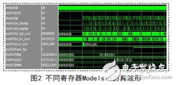
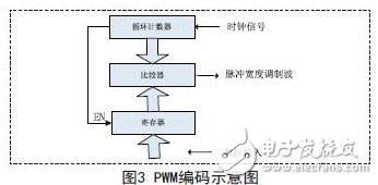
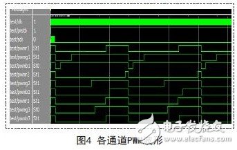
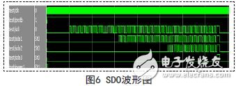
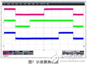
1 Introduction LED has developed rapidly in recent years due to its long use time, large viewing angle, high brightness, and colorful colors. It is the fourth generation of new energy after incandescent lamps, high-intensity discharge lamps and fluorescent lamps. LED is a P/N junction semiconductor. It is a solid-state cold light source. Compared with traditional light sources, it has the advantages of low power consumption, environmental protection, safety and reliability, and small size. In order to strengthen the goal of energy saving and emission reduction, it is an irresistible trend to add dimming function to various types of LED drivers. Generally, there are three types of LED driver dimming methods: thyristor dimming, analog dimming, and PWM (pulse width modulation) dimming. Each dimming method has its advantages and limitations. In order to facilitate digital signal control, the chip mainly uses pulse width modulation (PWM) to dim. Pulse width modulation (PWM) is one of the pulse modulation methods, which means that the operating frequency is constant (ie, the duty cycle is constant), and the duty cycle is changed by changing the on-time or off-time of the power switch. The duty ratio is the ratio of the time that the high level takes up within one cycle, and the output voltage is stabilized by the adjustment of the duty cycle. Widely used in many fields, from measurement and communication to power control and conversion and LED lighting. 2. Chip structure block diagram Figure 1 shows the block diagram of the dimming chip, where SDI is used to receive data, SDO is used for data backward transmission, the oscillator provides a clock crystal for the chip, VLED supplies power to the chip, and LDO is a linear regulator. The digital control unit includes a decode module and a PWM module, and OUTR, OUTG, and OUTB are three output terminals of the chip for color display. 3. How the chip works The chip uses a single-wire communication method to transmit data, and uses a return-to-zero code to transmit signals. After the system is powered on, the SDI receives the data stream transmitted from the controller. The data stream is binary data based on the return-to-zero code. When each chip receives 36 bits, the SDO output port starts to forward data to provide input for the next chip. data. RGB is a color standard in the industry, which is obtained by changing the three color channels of red (R), green (G), and blue (B) and superimposing them on each other. The three PWM outputs of the system OUTR, OUTG, and OUTB pass through the digital control unit, and each channel receives 12-bit data. Each channel has 12-bit PWM gray-scale control with 4096 gray levels. Each channel sends a signal with a different duty cycle. If the input is a RESET signal, the system sends the received data to the LED display. 4. Implementation of main function modules 4.1 decode module This module is used for data collection, determines whether the input data is 1 or 0, and transfers the data to the R, G, and B ports. Using the pulse edge detection method, the rising edge sdi_posedge and sdi_negedge signals of the input data are obtained, and the number of high-level clocks, the number of low-level clocks, and the number of clocks of the entire period of one data cycle are stored in three registers of high_count, low_count, and count_cycle, respectively. In the falling edge of the data, the data in the high_count register is compared with the data shifted to the right by the count_cycle register. When the value in high_count is greater than the value shifted by one bit in the counter_cycle, we determine the data entered at this time. Bit 1, and vice versa. 0. Store 0 or 1 at this time in the last bit of the 8-bit register data_reg. For each falling edge of data, add 1 to the sdi_negedge_count register. When the value of this register is 12, 24 respectively. At 365, 8 is the data in the register data_reg, and rdata, gdata, and bdata are used for the encoding of the PWM module. When sdi_negedge_count is 36, the frame_flag register is set to 1, indicating that the module has received the data, and the remaining signals are forwarded through SDO. Figure 2 shows the simulated waveforms of Modelsim for each register. 4.2 PWM module This module is used to encode the data collected by the decode module for PWM encoding and output waveforms with different duty cycles. In Figure 3, when a clock pulse comes, the output of the loop counter increases, the register latches a 12-bit signal, and the latch signal is continuously compared with the data of the loop counter. When the latch signal is smaller than the output of the loop counter, the comparator Output high level, otherwise output low level. After the loop counter loops for one cycle, an enable signal EN is issued to the register, and the register latches the next signal. In each counter counting period, the number of high levels outputted by the comparator output is different due to the different sizes of the input modulated signals, thus generating pulse width modulated signals having different duty ratios. Figure 4 shows the PWM waveforms for each channel. 5. Chip cascading verification and verification analysis The chip is cascaded by means of single-wire transmission. Its characteristic is: only one data line is used for signal transmission, which greatly reduces the size of the printed circuit board, reduces the difficulty of wiring, requires fewer peripheral devices, and improves the number of devices. Chip reliability and stability. Figure 5 shows the three cascaded working diagrams of the chip. The data enters the first chip from the left SDI, each chip intercepts 36 bits of data, and the remaining data is forwarded, and SDO1, SDO2, and SDO3 are the output data of the previous chip, respectively. After the RTL level code is written, the function simulation is performed with Modelsim, the logic synthesis is performed by Synopsys' DesignCompile, the static timing analysis is performed by the Prime TIme tool, and the automatic layout and routing is performed by Cadence's Silicon Ensemble. After the post-imitation test, the final completion is completed. Streaming. Figure 7 shows the oscilloscope test waveform after the completion of the tape. 6 Conclusion This paper uses the QuartusII platform to write RTL code, uses Modelsim simulation software to perform functional simulation, and finally uses the oscilloscope to test the real object, and obtains the ideal waveform, which basically meets the expected design requirements, and the corresponding RGB outputs the correct waveform. This article has basically completed the design requirements, but also needs to optimize the code to improve reliability and stability before it can be used for mass production. Aluminum core Solar Cable is a photovoltaic circuit using aluminum as a conductive material. It is widely used in solar power generation systems to transport the electricity generated by solar panels. Aluminum Solar Cable,Photovoltaic Solar Cable,TUV Aluminum solar cable,Aluminum Energy Cable Suzhou Yonghao Cable Co.,Ltd. , https://www.yonghaocable.com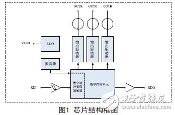

Compared with traditional copper solar cable, aluminum solar cable has some obvious advantages, the most important of which is low cost.
1. Low price: Aluminum is a common metal, and its price is cheaper than that of copper. Therefore, the use of aluminum solar cable can reduce the cost of the system and make the entire photovoltaic power generation project more economical.
2. Lightweight: Aluminum has a lower density and is lighter than copper. The aluminum core optical cable can reduce the weight of the cable and facilitate installation and maintenance.
3. Strong corrosion resistance: Aluminum has good corrosion resistance and can maintain a long service life under harsh environmental conditions. This makes the aluminum solar cable more reliable for outdoor use.
4. Excellent conductivity: although the conductivity of copper is higher than that of aluminum, the aluminum solar cable can make up for the shortcomings of the low conductivity of aluminum to a certain extent by optimizing the design and process and ensure the efficiency and stability of power transmission.
It should be noted that there are also some limitations and precautions for aluminum solar cable. Due to the low conductivity of aluminum, the resistance of the aluminum solar cable will be relatively high, so it is necessary to choose the wire diameter and length reasonably when designing and installing to ensure the efficiency of power transmission. In addition, aluminum is prone to electrochemical reactions when it comes into contact with copper, so corresponding measures need to be taken when connecting aluminum solar cable and other components, such as using special connectors or coating protective layers.
In general, aluminum solar cable with its low cost, corrosion resistance, light and other advantages, has been widely used in solar power generation systems, and brings economic and reliability benefits to photovoltaic power generation projects.