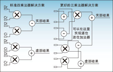
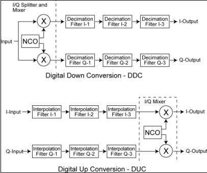
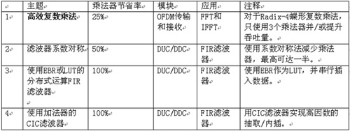
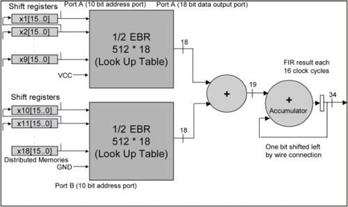
Label: FPGA Wireless Base Station This article refers to the address: http:// Emerging broadband wireless protocols based on WiMax and its derived standards require ever higher throughput and data rates. The fast chip rate and digital RF processing proposed by these protocols can be optimally implemented on hardware using FPGA solutions. FPGAs are well suited as high-performance, cost-effective solutions for implementing digital functions in these physical layer protocols because they include the following rich resources: 1. DSP module, can be used to implement the multiplier and adder/accumulator functions required for various FIR filtering and FFT/IFFT operations; 2. SERDES transceiver that supports CPRI and OBSAI interfaces between the wireless front end and the baseband digital board; 3. Important FPGA embedded RAM block memory (EBR), which can be used to store filter coefficients, perform block interleaving, and implement FEC decoding (Turbo, Viterbi, Reed-Solomon, etc.); 4. High speed LVDS I/O, supporting the DAC and the wide parallel interface from the ADC, respectively. These converters define the boundaries between RF/analog functions and inexpensive digital baseband logic. The higher the interface speed, the more cost-effective FPGA solutions can integrate more digital upconversion/digital downconversion. This article focuses on the first resource, the DSP multiplication module. By reducing and optimizing the implementation of the DSP multiply module in FFT and FIR, designers can meet throughput requirements while minimizing resource usage, allowing users to use the most cost-effective off-the-shelf FPGA devices. The four multiplier saving techniques are described below. Efficient complex multiplication for WiMaxOFDM functions An important feature of WiMax system design is the support for Orthogonal Frequency Division Multiplexing (OFDM). FPGAs make it particularly easy to implement OFDM transmitters and receivers in discrete time using IFFT and FFT, respectively. Protocols such as 802.16a require a 256-sample FFT. The 802.16e protocols require multiple FFT samples or flexible FFT samples to accommodate dynamic channel and bandwidth requirements (Scalable OFDMA). Complex multiplication The most efficient use of multipliers is achieved with the Radix-4 architecture when performing 256 and 1024 sample FFTs. The FFT algorithm is decomposed by multiplexing a 4-sample discrete Fourier transform (DFT) butterfly structure. For example, a 16-point FFT can be implemented with a 2-stage Radix-4 DFT structure by time extraction, frequency extraction, or other correlation decomposition. The first level consists of four 4-point DFTs, and the second level consists of four 4-point DFTs. Since the output of each DFT requires three phase factors to be provided for the result before being fed to the next stage, the nine phase factors between the first and second stages require nine complex multiplications. At first glance, performing a complex multiplication requires 4 multipliers and 2 adders/subtractors. However, the expression can be rewritten as another expression that requires only 3 multipliers, 3 adders, and 2 subtractors. It is worth noting that the adder is implemented in the core logic of the FPGA, using a rich general-purpose programmable logic unit (PLC) slice in a bit-by-bit carry mode. If D = Dr + jDi is complex data, C = Cr + jCi is a complex coefficient, then the standard expression of complex multiplication is as follows: E1: R = D * C = (Dr + jDi) * (Cr + jCi) = Rr + jRi (1) Where Rr=Dr*Cr-Di*Ci, Ri=Dr*Ci+Di*Cr The above standard expression requires the use of 4 multipliers. This expression can be rearranged by algebraic methods as: E2: Rr=Dr*Cr-Di*Ci (2) E3: Rr=Dr*Cr-Di*Ci+0 (3) E4: Rr=Dr*Cr-Di*Ci+(Dr*Ci-Di*Cr)-(Dr*Ci-Di*Cr) (4) E5: Rr=(Dr*Cr-Dr*Ci+Di*Cr-Di*Ci)+(Dr*Ci-Di*Cr) (5) The new expression for the plural result is: E6: Rr=[(Dr+Di)*(Cr-Ci)]+(Dr*Ci-Di*Cr) (3 times multiplication) (6) E7: Ri=Dr*Ci+Di*Cr (multiplied by the product of Rr) (7) As shown in Figure 1, the optimal complex multiplication can be implemented with 3 multipliers, 3 adders, and 2 subtractors. It is worth noting that in FPGAs, the relative die area used by the add/subtract module is less than the 18×18 multiplier block. Figure 1: Complex multiplication with 4 and 3 multipliers In summary, a 25% reduction in the number of multipliers used can lead to one of two major benefits: 1. Less multipliers can be used under the same FFT throughput conditions; 2. The FFT throughput can be improved under the condition that the number of multipliers is constant. Efficient implementation of FIR filter in digital upconverter/downconverter The following three high efficiency multiplier techniques can be used to implement digital upconversion and downconversion in an FPGA. This has become a key area of ​​optimization because wireless designers need to meet the requirements of moving data from very high sampling rates to chip processing rates. The Digital Downconverter/Upconverter (DDC/DUC) subsystem is the primary digital device for the transmitter/receiver in the base station and was previously implemented with expensive analog/mixed-signal devices. There are three techniques that can be used to reduce the number of multipliers in an FPGA implementation. 1. Symmetrical FIR filter saves multipliers; 2. Distributed arithmetic operations use embedded block memory; 3. The cascaded integral comb filter uses an adder. Upconversion/downconversion overview As described in the upper part of Figure 2, the DDC consists of a numerically controlled oscillator (NCO)-based I/Q splitter that uses sine and cosine inputs from the RF section through two mixers. The wave is modulated; a decimation section can be configured by a 3-stage FIR decimation filter or an FIR decimation filter followed by a cascaded integrator comb (CIC) filter. Figure 2: DDC/DUC structure The DUC in Figure 2 consists of a 3-level FIR interpolation filter or a CIC filter followed by an FIR interpolation filter; an I/Q mixer based on NCO and two mixers, which is at I The Q output signals are demodulated before they reach the RF section. Keep in mind that the extraction is used for sample deletion to achieve a lower sample rate, while the interpolation is used to increase the extrapolated sample to increase the sample rate. General implementation guide for frequency converters The DDC/DUC system is a system that requires a large number of multipliers. The decimation and interpolation filters are usually implemented by a multiplier and adder array, and the mixing function is a multiplier. The use of the area optimization method to implement the NCO is based on the phase shift using a complex multiplier. The challenge of overcoming systems that require a large number of multipliers is first to decompose and cascade filters: 1. A large FIR decimation filter or FIR interpolation filter with a decimation/interpolation factor of N can be decomposed into two or three smaller, simpler stages with decimation/interpolation coefficients of N1, N2 and N3, respectively. Connected filter. The extraction/interpolation coefficients satisfy the following equation: E8: N=N1*N2*N3 2. Decomposing the FIR decimation filter or the FIR interpolation filter into two or three independent filters reduces the total number of taps required to implement the entire filter. A single filter that extracts or interpolates a factor of N requires a large number of taps (multipliers) to meet the basic filter attenuation and noise characteristics requirements. Decomposing the filter into two or three smaller and simpler filters can reduce the number of taps throughout the filtering system. In addition, the lower sampling rates of the second and third cascaded filters can achieve time multiplexing, further reducing the size of the implementation. When the filter order is determined, various measures can be taken to reduce the number of multipliers in the actual filter. This will be described below. Table 1: Four techniques to reduce the number of multipliers in WiMax system design Three multiplier saver technologies dedicated to frequency converters Symmetric extraction and interpolation filter Coefficient-symmetric DDC decimation filters and DUC interpolation filters can be used to achieve multiplier savings of up to 50%. Under symmetric conditions, the n-tap FIR filter coefficients h(0), h(1), ..., h(n) satisfy h(k)=h(nk){0≤k≤n}. Since the product of h(k) = h(nk), h(k) and the sum of two related samples can be done at one time, the number of multipliers required can be reduced by a factor of at most 2 (for even coefficients). In an FPGA, the addition of two data samples using the same coefficients can be implemented using low cost bit-wise carry logic. 2. Implement FIR filter by distributed computing function and using EBR memory block For multiplier-intensive applications such as DDC or DUC, efficient use of FPGA resources is especially important. Using memory and LUT structure resources as multipliers can significantly improve implementation efficiency. EBR and distributed memory of this structure can be used as FIR filter multipliers using distributed memory technology. Distributed memory technology, also known as soft multiplication, typically increases the number of multipliers in an FPGA device by a factor of two to five. It can be seen from Figure 3 how to implement an FIR filter using distributed arithmetic techniques using EBR. The sample is serially shifted into the EBR address bus. Inside the EBR there is a pre-computed result multiplication table and the sum of the individual input sample bits (address bits) with appropriate coefficients. The accumulator will accumulate n (n is the sample bit resolution) intermediate result and provide a complete FIR filtering result after n clock cycles. Figure 3: Using block memory as an FIR multiplier 3. CIC filter uses adder instead of multiplier Replacing some of the interpolated/decimated FIR filter chain portions with a CIC multiplier is another way to reduce the number of multipliers required to implement. The CIC multiplier does not require a wide range of rate changes in hundreds of steps. High rate variation interpolation or decimation filters are very expensive in terms of hardware. The CIC filter, also known as the Hogenauer filter, can be used as a low-cost, high-factor extraction or interpolation filter. They can be used to achieve arbitrary and large rate changes in digital systems and can be efficiently implemented using only adders and subtractors. Because FPGAs have a very fast carry chain for implementing adders, CIC filters are well suited for FPGA implementations. See Table 2 for the structure and characteristics of the integrator and comb filter. Table 2: Structure and characteristics of comb filters and integrators Realize inverter and OFDM with IP core Implementing DDC or DUC drives with Lattice's FPGAs is fairly straightforward because FPGAs provide an important component for use as an IP core. The use of a CIC filter as an interpolator in data rate conversion is illustrated in Figure 4, which shows the use of a CIC interpolator for use as a frequency converter in digital wireless applications. Figure 4: Digital Upconverter for Digital Radio Applications The digital upconverter uses the following IP core configurations: 1. FIR filter (63-tap interpolation filter); 2. FIR filter (31 tapped interpolation filter); 3. CIC filter (interpolated CIC filter programmable at a rate between 8 and 2K); 4. NCO (NCO with sine and cosine outputs). Advantages of LatticeECP2/M The LatticeECP2/M family of low-cost FPGAs offers a wide range of high performance features that are highly relevant to WiMax system design. These features are difficult to find in other low-cost FPGA family devices and can only be found in expensive high-end FPGA products: 1. High-performance DSP blocks with hardwired multipliers, adder/accumulator modules, and pipeline stages; 2. SERDES transceiver channels up to 3.125 Gbps, supporting CPRI and OBSAI interfaces between the radio head and baseband digital boards; 3. A large number of 18kB EBR memory blocks in the LatticeECP2/M memory enhancement family; 4. High-speed LVDS I/O supporting ADC/DAC interface, input and output rates up to 840Mbps; 5. The low-cost LatticeECP2/M family of devices delivers these rich and high-performance resources at a fraction of the price of other FPGA devices. WiMax system designers can also use a variety of design techniques to reduce the number of DSP multipliers required, making it possible for users to use smaller, cheaper FPGA devices. Customized Plug adaptor charger fast charger, usb c adapter, usb-c charger TOPNOTCH INTERNATIONAL GROUP LIMITED , https://www.itopnoobluetoothes.com