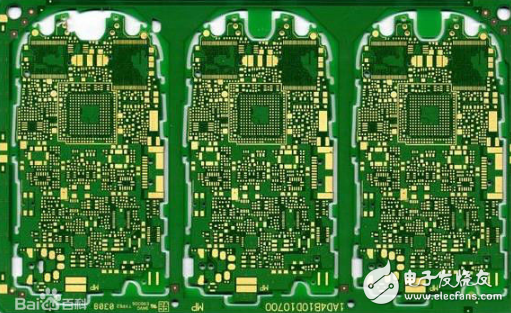
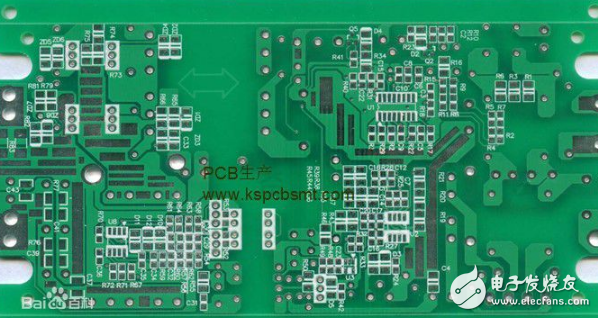
PCB (PrintedCircuitBoard), Chinese name is printed circuit board, also known as printed circuit board, is an important electronic component, is the support of electronic components, is the carrier of electrical connection of electronic components. Because it is made by electronic printing, it is called a "printing" circuit board. PCB production process: 1, contact the manufacturer First you need to contact the manufacturer, then register the customer number, then someone will quote you, place an order, and follow up the production schedule. Purpose: According to the requirements of the engineering data MI, cut into small pieces on the large sheet that meets the requirements. Small pieces of sheet that meet customer requirements. Process: large sheet material → cutting board according to MI requirements → seesaw → beer fillet \ edging → exit board 3, drilling Purpose: According to the engineering data, the required aperture is drilled at the corresponding position on the sheet of the required size. Process: stacking pin → upper plate → drilling → lower plate → inspection \ repair 4, sinking copper 2. Objective: The copper is deposited by chemically depositing a thin layer of copper on the walls of the insulating holes. Process: rough grinding → hanging board → copper line automatic line → lower board → dip % dilute H2SO4 → thick copper 5, graphics transfer Purpose: Graphic transfer is the transfer of images on the production film to the board Process: (blue oil process): grinding board → printing the first side → drying → printing the second side → drying → explosion → shadowing → inspection; (dry film process): hemp board → laminating → standing → right Bit → Exposure → Rest → Shadow → Check 6, graphic plating Purpose: Graphic plating is to electroplat a layer of copper on the exposed copper skin or hole wall to a desired thickness of copper layer and a desired thickness of gold or tin. Process: upper plate → degreasing → water washing twice → micro-etching → water washing → pickling → copper plating → water washing → pickling → tin plating → water washing → lower plate 7, unwinding 2. Objective: Retreat the anti-plating coating layer with NaOH solution to expose the non-line copper layer. Process: water film: inserting → soaking alkali → washing → scrubbing → passing machine; dry film: placing board → passing machine 8, etching Purpose: Etching is the use of chemical reaction method to corrode the copper layer in non-line parts. 9, green oil Purpose: Green oil transfers the pattern of green oil film to the board to protect the line and prevent tin on the line when soldering parts. Process: grinding plate → printing photosensitive green oil → 锔 plate → exposure → shadow; grinding plate → printing the first side → baking sheet → printing the second side → baking sheet 10, characters Purpose: Characters are provided as an easy-to-identify mark Process: After the end of green oil → cool and cool → adjust the network → print characters → after 锔 High Voltage STA Armored Cable High Voltage STA Armored Cable,PVC Sheathed Electric Cable,Copper Conductor Power Cable,High Voltage Xlpe Power Cable Ruitian Cable CO.,LTD. , https://www.hbruitiancable.com

First, PCB printed circuit board