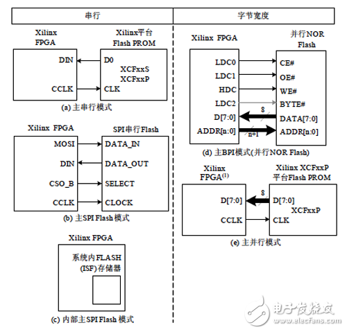
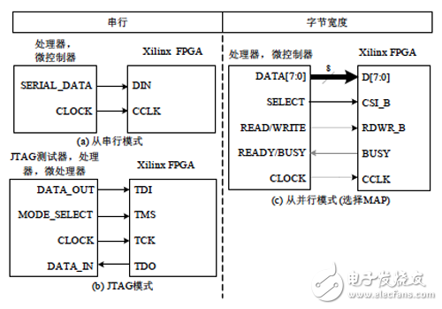
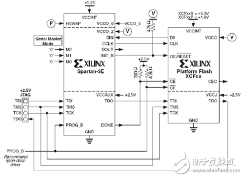
The FPGA configuration mode is flexible, and the main data, the slave mode, and the JTAG mode are classified according to whether the chip can actively load the configuration data by itself. The typical master mode is to load the configuration bitstream in an off-chip nonvolatile (power-down data-free) memory. The required clock signal (called CCLK) is generated internally by the FPGA and the FPGA controls the entire configuration process. The slave mode requires external master intelligent terminals (such as processors, microcontrollers, or DSPs) to download data to the FPGA. The biggest advantage is that the FPGA configuration data can be placed in any storage location of the system, including: Flash, hard disk. , network, and even in the running code of the rest of the processor. The JTAG mode is debug mode, which can download the bit file stream from the PC to the FPGA and lose it when power is off. In addition, Xilinx currently has an Internet-based, proven Reconfigurable Logic System ACE solution. (1) Main mode In the main mode, after the FPGA is powered on, the configuration data is automatically read from the corresponding external memory into the SRAM to realize internal structure mapping; the main mode can be further divided into: serial mode according to the bit width of the bit stream (single bit stream) ) and parallel mode (byte width bitstream) two major categories. Such as: main serial mode, main SPI Flash serial mode, internal main SPI Flash serial mode, main BPI parallel mode and main parallel mode, as shown in Figure 5-19. (2) slave mode In the slave mode, the FPGA acts as a slave device, and the timing required for configuration is provided by the corresponding control circuit or microprocessor to implement the download of the configuration data. The slave mode is also divided into two types according to the bit width of the bit stream, and the mode includes: serial mode, JTAG mode, and parallel mode. The summary is shown in Figure 5-20. (3) JTAG mode In JTAG mode, the clock communicated between the PC and the FPGA is the TCLK of the JTAG interface, and the data enters the FPGA directly from the TDI to complete the configuration of the corresponding functions. Figure 5-19 Schematic diagram of the common main mode download mode Figure 5-20 Schematic diagram of the commonly used slave mode download mode At present, mainstream FPGA chips support various common master and slave configuration modes and JTAG to reduce the impact of configuration circuit mismatch on the overall system. In the main configuration mode, the FPGA generates its own clock and loads the configuration data from the external memory. The bit width can be single bit or byte. In the slave mode, the external processor passes the synchronous serial interface according to the bit or word. The section width feeds the configuration data to the FPGA chip. In addition, multiple FPGAs can share the same external memory in JTAG daisy chain. The same piece/multiple FPGAs can also read configuration data and user-defined data from multiple external memories. There are five common configuration modes for Xilinx FPGAs: main string mode, slave string mode, Select MAP mode, Desktop configuration, and direct SPI configuration. In the slave string configuration, the FPGA receives configuration bit data from an external PROM or other device, and performs configuration under the action of the clock CCLK generated by the FPGA. Multiple FPGAs can form a daisy chain to acquire data from the same configuration source. The configuration data in the Select MAP mode is parallel and is the fastest configuration mode. The SPI configuration is primarily used in FLASH circuits with SPI interfaces. The Spartan-3E series chip is taken as an example to give various configuration circuits. In the main string mode, the working clock is supplied to the PROM by the CCLK pin of the FPGA, and the corresponding PROM sends data from the D0 pin to the DIN pin of the FPGA on the rising edge of CCLK. Regardless of the PROM chip type (even if it supports parallel configuration), only its serial configuration function is utilized. Figure 5-21 shows the single-chip main string configuration circuit of the Spartan3E series FPGA. The main string mode is the simplest and most common way of Xilinx's various configuration methods. Basically all programmable chips support the main string mode. Figure 5-21 Spartan-3E main string mode configuration circuit The three most critical points of the main string configuration circuit are the integrity of the JTAG chain, the setting of the supply voltage, and the consideration of the CCLK signal. As long as there is a problem in any of these 3 steps, the PROM chip cannot be properly configured. (1) JTAG chain integrity Both the FPGA and the PROM chip have their own JTAG interface circuits. The so-called JTAG chain integrity refers to the TMS and TCK of the JTAG connector, FPGA, PROM, and is guaranteed to form from the JTAG connector TDI to its TDO. JTAG connector "TDI → (TDI ~ TDO) → (TDI ~ TDO) → JTAG connector TDO" closed loop, where (TDI ~ TDO) is a pair of input and output pins of the FPGA or PROM chip itself. The JTAG chain of the configuration circuit in Figure 5-12 forms the complete JTAG chain from the TDI of the connector to the TDI of the FPGA, from the TDO of the FPGA to the TDI of the PROM, and finally from the TDO of the PROM to the TDO of the connector. Known as the chain head chip. You can also change the position of the FPGA and PROM as needed to make the PROM the first chip. (2) Power adaptability Industrial and Medical Display
There are many kinds of LCD classification standards, which can be divided into passive matrix and active matrix according to the driving mode
Passive matrix: Passive matrix LCD can be divided into TN-LCD(TwistedNematic LCD), STN-LCD(SuperTN-LCD) and DSTN-LCD(Doublelayer STN-LCD).
Active matrix: Active matrix LCD, also known as TFT-LCD, is widely used at present. Tft-lcd is short for thin-filmliquid-Crystal Display
The TFT-thin Film Transistor
Liquid Crystal Display
Short for TFT-LCD Liquid-CrystalDisplay
Tft-lcd has been widely used in various display equipment due to its advantages of small size, light weight, low radiation, low power consumption and full color.
Functions of TFT-LCD structure
(1) Backlight plate module: provide the source of light;
(2) Upper and lower polarizing plates, TFT Glass Substrate, liquid crystal: forming polarized light, controlling the passage of light;
(3) Color filters: Provide TFT LCD red, green and blue (three primary colors of light) sources;
(4) ITO transparent conductive layer: provide transparent conductive path;
(5) Photo Spacer: Provide a fixed height for color filters and TFT Glass Substrate. As a space for liquid crystal infusion, and as a support for the upper and lower Glass layers.
Medical Display,Medical Lcd Monitor,Medical Monitor,Medical Grade Monito Tonya Display Limited , https://www.tydisplay.com

