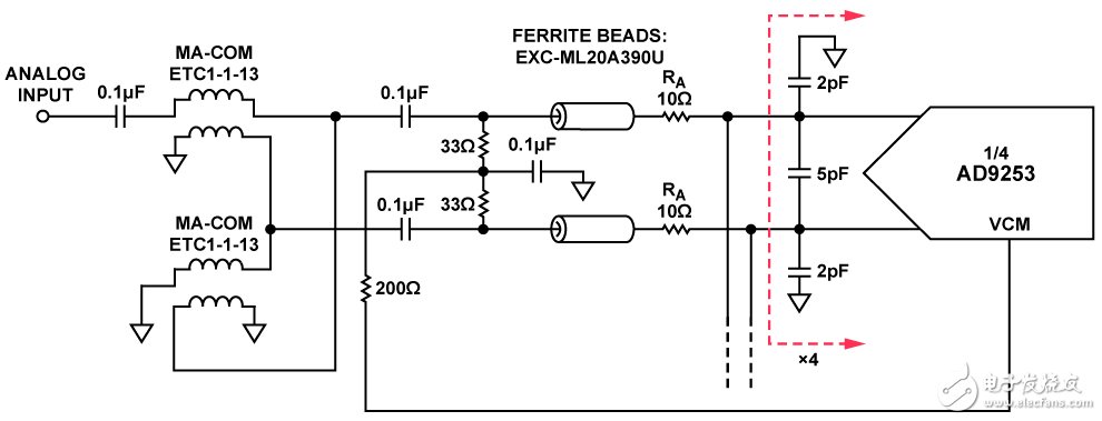
Circuit function and advantage The circuit shown in Figure 1 is a simplified diagram of a 14-bit, 125 MSPS four-channel ADC system that uses a back-end digital summation to boost the signal-to-noise ratio (SNR) from 74 dBFS for a single-channel ADC to 78.5 dBFS for a four-channel ADC. This technology is ideal for applications that require high SNR (such as ultrasound and radar) and utilizes modern high performance, low power, quad pipelined ADCs. This circuit uses the basic principle that the uncorrelated noise sources are added on a square and root (rss) basis, and the signal voltages are added on a linear basis. Figure 1. Basic block diagram of four parallel ADC summations for higher SNR Circuit description The input to each ADC consists of a signal term (VS) and a noise term (VN). The four noise voltage sources are summed to obtain the total voltage VT, which is the linear sum of the four signal voltages plus the four noise voltage squares and roots, for example: Since VS1 = VS2 = VS3 = VS4, the signal can be effectively multiplied by 4, and the converter noise - with the equivalent rms value - is multiplied by 2, so the signal-to-noise ratio is increased by a factor of 2, which is 6.02 dB. Therefore, an SNR increment of 6.02 dB is the result of an additional effective resolution bit caused by summing four similar signals. Since SNR(dB) = 6.02N + 1.76 dB, where N is the number of bits, Table 1 shows the theoretical SNR values ​​obtained by summing multiple ADC outputs. For convenience, it is obvious that you should choose to sum the four ADCs. In some critical cases, more ADC summation may be required, depending on other system specifications (including cost) and available board space. Table 1. Increased SNR vs. Number of ADCs Number of ADCs SNR Increment (dB) The ideal SNR for a 14-bit ADC is (6.02 &TImes; 14) + 1.76 = 86.04 dB The typical SNR specified in the AD9253 data sheet is 74 dB, but it produces an ENOB of 12 bits. The circuit shown in Figure 1 integrates a passive receiver front end consisting of four analog input channels using a 14-bit, 125 MSPS four-channel analog-to-digital converter, the AD9253. The circuit accepts a single-ended input and converts the input to a differential signal through a wide bandwidth (3 GHz) M/A-COM ETC1-1-13 balun with a 1:1 impedance ratio in a double-balanced configuration, as shown in Figure 2. Show. Figure 2. Input analog summation network All four ADC inputs are connected on the secondary side of the balun configuration. There is no gain in the circuit, and each analog input pair has a simple filtering function that reduces the residual kickback signal that may be fed back to the adjacent ADC channel. Planar Die Construction Sealed Glass Case Ideally Suited for Automated Insertion - 75V Nominal Zener Voltages MELF Changzhou Changyuan Electronic Co., Ltd. , https://www.cydiode.com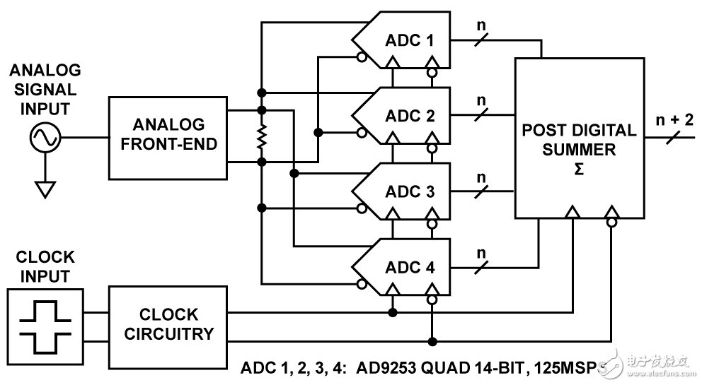
![]()
![]()

![]()
Case: MiniMELF, Glass Terminals: Solderable per MIL-STD-202, Method 208 Polarity: Cathode Band Approx. Weight: 0.05 grams
= 25°C unless otherwise specified Symbol Pd VF RqJA Tj, TSTG Value to +175 Unit mW V K/W °C
Characteristic Forward Voltage = 200mA Thermal Resistance, Junction to Ambient Air (Note 2) Operating and Storage Temperature Range Notes:
1. Tested with Pulses, 20ms. 2. Valid provided that Electrodes are kept at Ambient Temperature.
1. Tested with pulses = 20 ms. 2. Valid provided that electrodes are kept at ambient temperature.
VZ, ZENER VOLTAGE (V) Fig. 1, Zener Current vs Zener Voltage
25 20 VZ, ZENER VOLTAGE (V) Fig. 8, Zener Current vs Zener Voltage
TA, AMBIENT TEMPERATURE (°C) Fig. 3, Power Dissipation vs Ambient Temperature
15 20 VZ, ZENER VOLTAGE (V) Fig. 4, Differential Zener Impedance
VZ, ZENER VOLTAGE (V) Fig. 5, Junction Capacitance vs Zener Voltage