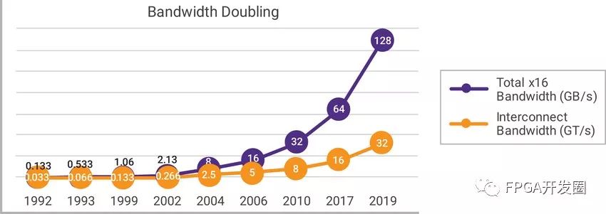
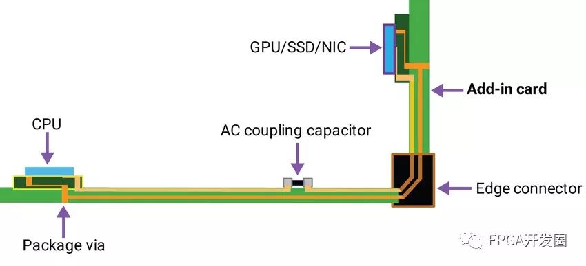
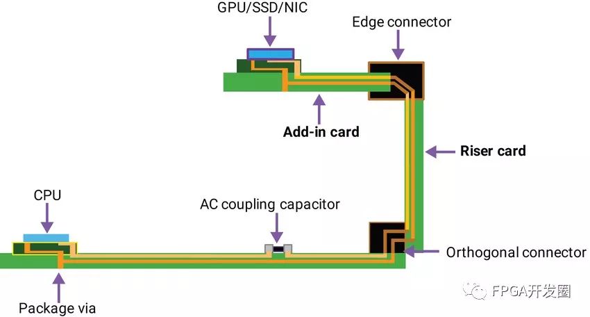
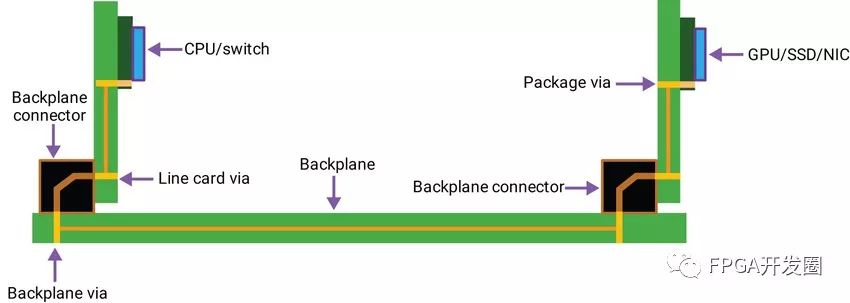
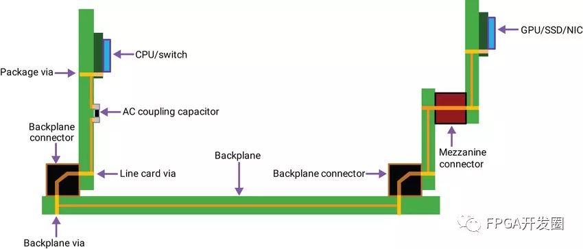
The use of PCI Express® (PCIe) interfaces is common in computing and networking applications. These applications include central processing units (CPUs), graphics processors (GPUs), network interface cards (NICs), switches, servers, and devices such as solid state devices (SSDs). ) Newer types of storage systems, and so on. However, today's networks and rapidly emerging artificial intelligence (AI) applications require greater bandwidth and faster interconnects in accelerators and GPUs to send and receive larger amounts of data. Given the widespread use of PCIe in such applications and the increasing bandwidth requirements, the PCI-SIG Industry Alliance recently announced the latest specification, PCIe 5.0, which increases the data rate to 32GT/s and doubles the link bandwidth. , from 64GB/s to 128GB/s. Figure 1 shows the evolution of the PCIe interconnect and total bandwidth. Figure 1: PCI-SIG Bandwidth Growth The PCIe 5.0 specification mainly deals with speed improvements and modifications of the related physical layer (PHY layer). However, moving to the 32GT/s design will bring several challenges that system designers and PHY designers must consider. This article describes the challenges of transitioning to PCIe designs at 32 GT/s, and how designers can successfully design systems using the new PCIe 5.0 interface. System Designer Challenges Printed circuit board (PCB) traces, connectors, cables, and even IC packages are system-wide bandwidth limiting factors that make high-data-rate designs challenging. High signal frequencies increase copper losses and power losses, which can result in reduced transmission distances. In addition, channel loss in higher signal frequencies can cause signal integrity (SI) problems. In order to meet the requirements of various applications, there are many types of PCIe channels, ranging from "chip-to-chip" topologies that do not include connectors, to complex server topologies that include backplane interfaces, and such backplane interfaces include many PCB cards and two or more connectors. As shown in Figures 2 to 5, most PCIe lanes consist of one IC package on each end and have multiple PCBs, including: processor boards, add-in cards, and riser cards; all of them are connected to one or Multiple mezzanine cards or PCIe card electromechanical (CEM) connectors. Figure 2: "Chip-to-Chip" interface, the simplest channel, no connector Figure 3(a): Channel with a Mezzanine Connector Figure 3(b): Channel with one edge connector (additional card) Figure 4(a): Channel with Two Connectors and Using One Riser Card and One Add-on Card Figure 4(b): Standard Backplane Channel with Two Line Cards and Two Connectors Figure 5: Complex backplane channel with more than two connectors Historically, PCIe system designers have used general low-cost FR4 PCB materials and wirebond packages for most applications up to 8 GT/s data rate (Gen3), and this has proven successful. However, using this material and package at a data rate of 32 GT/s is not feasible. Due to increased channel loss, even in PCIe 4.0 with a maximum rate of 16 GT/s (which is essential for maintaining existing channel lengths in next-generation board designs), most designers are also working on FR4 PCBs. Turn to lower-loss materials such as MEGTRON. PCBs can also be designed with wider space spacing between traces to further increase system-level SI performance. Similarly, for SI, many designs will use enhanced CEM connectors or custom mezzanine connectors, and PCB vias will be drilled back to minimize the stub length. In some cases where the channel is very long, you can also use the retimer. However, all these enhancements come at a price. MEGTRON materials may cost 1.2 to 2.5 times more than standard FR4 materials, and PCB traces may require further spacing to achieve better jitter performance, resulting in larger, more expensive PCBs. If you use a stub back drill (an incremental step in the board manufacturing process), you will also increase the total cost of the PCB. Another factor to consider is how enhanced and customized surface mount connectors are more expensive than standard through-hole CEM connectors. In addition, the use of clock redrivers increases bill of materials (BOM) costs, data path delays, and system power consumption; they also occupy additional areas on the PCB, which increases board and assembly costs. To verify its design, system designers must work closely with signal integrity engineers, package designers, SoC designers, and board layout designers to model each component in its channel and verify its entire end-to-end performance. PHY Designer Challenges Progressive improvements to the 16GT/s PHY design are not sufficient for PCIe 5.0 channel requirements in most applications. Due to the significant increase in channel loss at 32 GT/s, the equalization circuits in the transmitter (TX) and receiver (RX) require significant improvements. In addition, more stringent jitter parameters and jitter limits and return loss specifications also require many sub-circuits to be redesigned in TX and RX. It is expected that the PHY of PCIe 5.0 will support channel margining through the controller and separate reference clock independent spread spectrum timing (SRIS). Please retain the English description and other functions while satisfying the process, voltage, and temperature corner recommendations. Keep strict timing and jitter requirements in English and other aspects. Such enhancements and additional limitations make the design of the PCIe 5.0 32GT/s PHY very complex and require many capabilities to achieve low power, small area, and low latency PHY while providing the best signal and power integrity (PI )performance. The accurate model, silicon-proven PHY allows designers to model, design, and simulate end-to-end channels for verification and optimization of system designs. summary In data-intensive applications such as networking, storage, and emerging artificial intelligence, the demand for bandwidth is increasing, which necessitates faster interconnections, such as the new PCIe 5.0 technology at 32 GT/s. However, designers must understand and consider the many challenges faced in moving to the 32GT/s PCIe design. Solving signal integrity, encapsulation, and channel performance issues at higher data rates requires full capabilities in multiple areas. This is why more and more system-on-chip (SoC) designers use proven third-party IP for successful IC integration. Many businesses are leveraging reliable and proven third-party IP and power integrity services such as Synopsys. With Synopsys' PCIe 5.0-based IP based on decades of PCIe expertise, SoC designers can start their 32GT/s designs as early as possible. SoC designers can work with Synopsys to discuss the performance requirements of PCIe lanes at higher data rates while addressing IP integration, timing closure, signal integrity, packaging, and manufacturing requirements. We will elaborate on each challenge in the document that will be released later. Shenzhen ChengRong Technology Co.,Ltd. , https://www.dglaptopstandsupplier.com