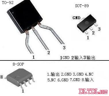
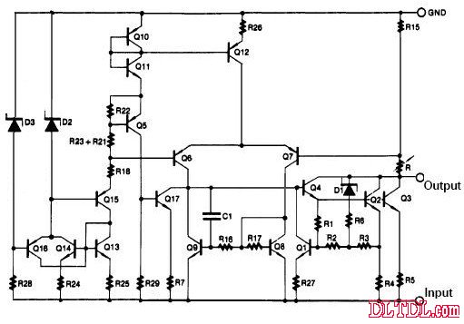
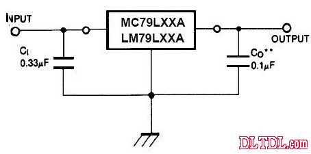
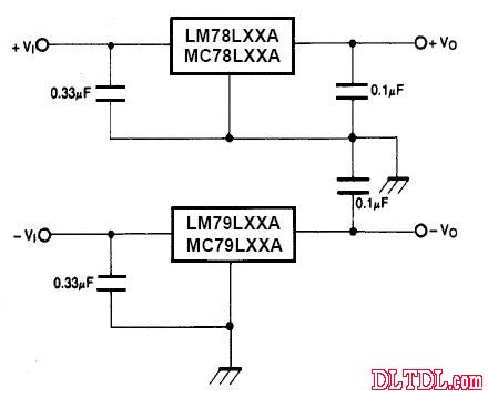
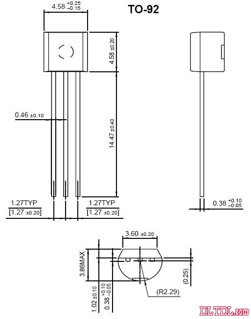
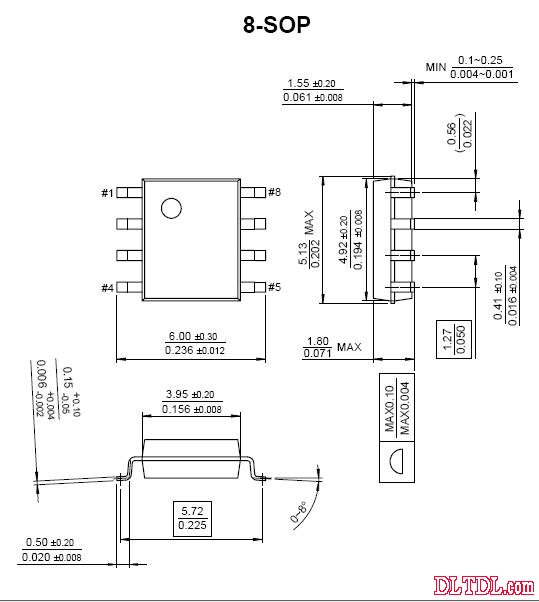
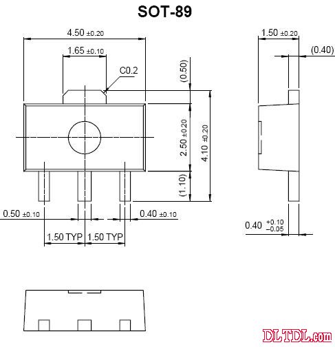
LM79L05A Chinese information introduction Electrical Characteristics Electrical Characteristics (MC79L05A/LM79L05A KA79L05) (VI=-10V, IO=40mA, CI=0.33ìF, CO=0.1μF, 0°C≤TJ≤+125°C, unless otherwise specified unless otherwise stated) Parameter parameter Symbol Symbol Conditions Test condition minimum typical maximum unit Output Voltage Output voltage VO TJ=+25 °C - 4.8 - 5.0 - 5.2 V Line Regulation Linear adjustment rate (Note1) ΔVO TJ=+25 °C -7.0V≥VI≥-20V - 15 150 mV -8V≥VI≥-20V - - 100 mV Load Regulation Load regulation (Note1) ΔVO TJ=+25 °C 1.0mA ≤ IO ≤ 100mA - 20 60 mV 1.0mA ≤ IO ≤ 40mA - 10 30 mV Output Voltage output Voltage VO -7.0V≥VI≥-20V, 1.0mA ≤ IO ≤ 40mA - 4.75 - - 5.25 V VI=-10V, 1.0mA ≤ IO ≤ 70mA - 4.75 - - 5.25 V Quiescent Current Quiescent current IQ TJ=+ 25 °C - 2.0 5.5 mA TJ=+125 °C - - 6.0 Quiescent Current Change quiescent current change with line ΔIQ -8V≥VI≥-20V - - 1.5 mA with load ΔIQ 1.0mA ≤ IO ≤ 40mA - - 0.1 mA Output Noise Voltage Output noise Voltage VN TA=+25°C, 10Hz ≤ f ≤ 100KHz - 30 - μV Ripple Rejection Ripple suppression RR f=120Hz, -8V≥VI≥-18V TJ=+25°C 41 60 - dB Dropout Voltage Voltage difference VD TJ= +25°C - 1.7 - V Note 1. Load and line regulation are specified at constant junction temperature. Change in VO due to heating effects must be taken Into account separately. Pulse testing with low duty is used. LM79L05A pin diagram and function Limit parameters: Parameter parameter Symbol Symbol Value Value Input Voltage Input voltage (for VO = -5V, -8V) VI-30V (for VO = -12V to -18V)-35 (for VO = -24V)-40Operating Junction Temperature Range Working range TJ0~ +125°CStorage Temperature Range Storage temperature range TSTG-65~ +150°C Figure 1 LM79LXXX pin layout LM79L05A circuit diagram introduction: Figure 2 LM79LXXX internal circuit diagram Figure 3 LM79LXXX typical test circuit diagram Figure 4 positive and negative voltage symmetrical output circuit Figure 5 LM78LXXX TO-92 package picture Figure 6 LM78LXXX 8-SOP SMD Package Picture Figure 7 LM78LXXX SOT-89 SMD Package Picture The high-current slip ring is specially developed for high-power equipment. It can choose 50A, 100A, 250A, 500A, 1500A, 3000A and other specifications. It can also combine current and signal, which is easy to install, light weight and large current load. It is very suitable for welding, electroplating and other industries. High Current Slip Ring,Encoder Servo Motor,Connector Electrical,Rotating Electrical Connectors Dongguan Oubaibo Technology Co., Ltd. , https://www.sliprob.com