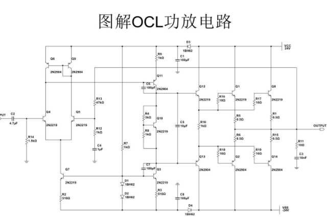
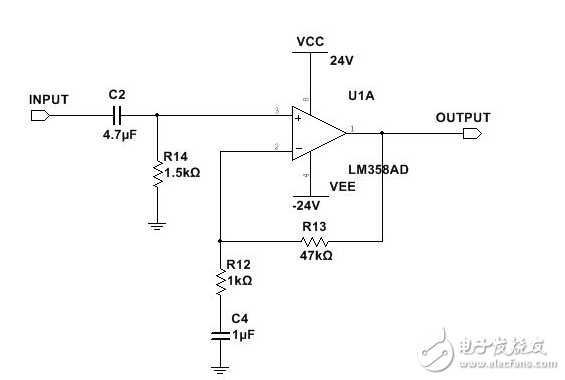
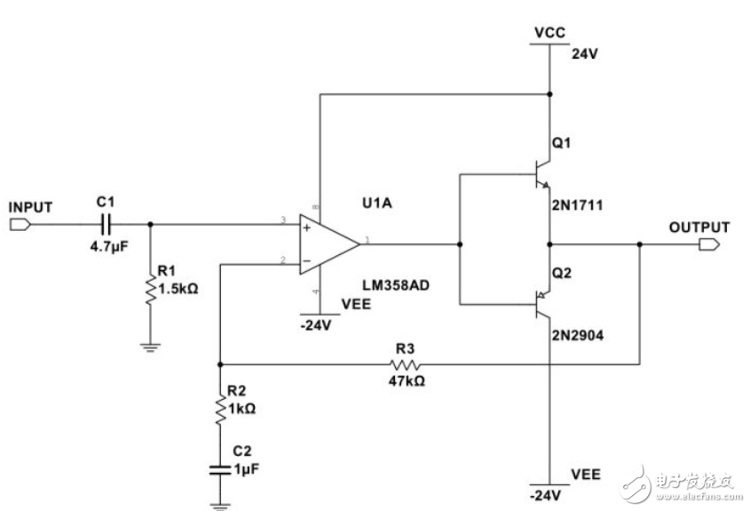
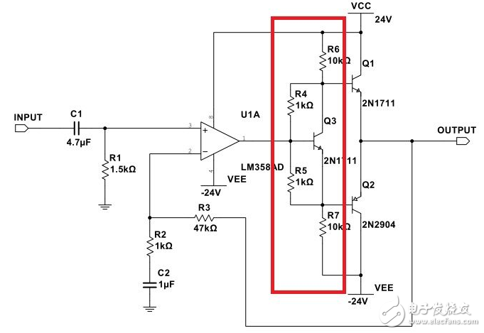
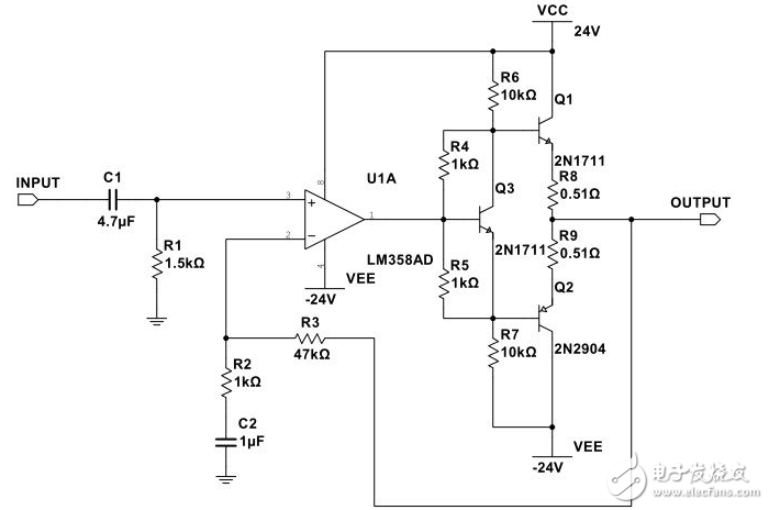
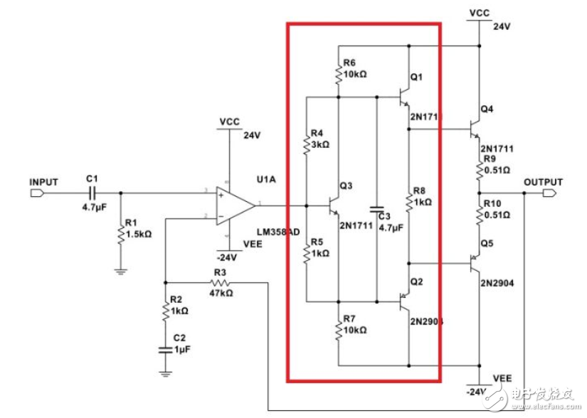
The subject of this paper is an OCL differential power amplifier that illustrates a classical circuit. This analysis can effectively reduce the fear of facing complex circuits. The entire OCL circuit can be equivalent to a high-power op amp, how to eliminate the crossover distortion of high-power transistors. How to limit the static bias current of Q1Q2 by adding a feedback resistor. To get more power, you can do it by juxtaposing power tubes. Let's explain some of the classic circuits in detail and make progress with everyone. In addition, although I have already turned to software, but the love of hardware will not be reduced, please rest assured. Friends have any classic circuit to understand or privately trust me. If there are more interested people, I will squeeze time to write a separate article to explain. Your support is the driving force for me to move forward. Just got it. (At the end of the writing, you have to breathe hard, ask for praise, and ask for comfort.)) Well, not much nonsense, the first phase of the schematic circuit diagram series, we explain a very classic OCL differential power amplifier circuit. The friends who learn the simulation know that the first small work of most newcomers to the simulation is basically the power supply, the power amplifier, these relatively simple, more practical circuits. Therefore, the first circuit here chose this classic power amplifier circuit. Look at the picture. (Figure 1 complete OCL differential amplifier circuit) Seeing this circuit diagram, maybe some of the friends who just started will be a bit blind. Don't be afraid, as long as you meditate on OCL Dafa, you can understand it. Haha, just kidding. Now let everyone bring together to analyze this circuit. My approach is from simple to difficult, from the framework to the details of the order to explain the circuit, first talk about the framework, and then gradually add circuit details, so everyone keep up with the idea. (Figure 2 OCL equivalent circuit) Yes, the circuit above, the entire OCL circuit can be equivalent to a high-power op amp, plus several resistors and capacitors constitute a co-directional amplifier, it is as simple as that. In order to facilitate understanding, I have mapped the number of resistors and capacitors in the equivalent circuit to the original picture. Do you see the difference and the connection? So how is the gain of the entire amplifier? What is the cutoff frequency? Is not it simple? What, you don't know the op amp? Come and come, open the computer, open the browser, call up the dog input method, and enter the "Tsinghua University analog electronic technology foundation", first look at it from the beginning. What, you can't read? Ok, go out and turn right. There are still bricklayers on the construction site. Go and sign up. I am not in a hurry after my brother! Well, if you can understand the equivalent circuit above, then you will understand this OCL circuit. Of course, in addition to a specific implementation details, you need to explain it. Come and come, we will restore the complete circuit above step by step. (Figure 3 uses a totem pole to increase output power) As shown above, add a level of totem pole to the rear stage of the op amp to increase the output power of the amplifier. What do you ask me as the two transistors Q1 behind Q, Q2 is called a totem pole? Oh, the ghost knows, maybe because the totem symbolizes strength, these two triodes give you strength. The little-eyed partner began to complain. Pro, your circuit is unscientific. The two bases of the back totem pole are directly connected together and there will be crossover distortion. That's right, boy. There is indeed crossover distortion. We have to ensure that the two triodes are always on. What should we do? Of course, the two transistors are provided with a paranoid voltage that maintains conduction. Look at the picture below. (Figure 4 eliminates the crossover distortion of the power transistor by adding a bias voltage) At this time, someone started to spit out, I added the bias voltage, but added a triode Q3 to provide the bias? Haha, this is going to say this legendary voltage doubler circuit. We only look at Q3, R4, R5, please tell me what is the voltage between the emitters of Q3? If the base current of the triode is ignored, is Vce=Vbe*(R4/R5+1) right? So if we change R4 to a potentiometer, can we adjust the voltage across Q3? This adjustable voltage is provided to Q1 and Q2 as a bias voltage. Of course, because the triode IC-Vbe transmission characteristic curve is very steep, the bias voltage is slightly larger, the collector current will rise, so in order to adjust the bias voltage more conveniently, we will be between the Q1 and Q2 emitters. Connect a small feedback resistor in series as shown below. R8, R9 as the emitter feedback resistor to maintain Q1, Q2 no-load bias current on a relatively small magnitude, reduce no-load power consumption, reduce heat. (Figure 4 limits the static bias current of Q1Q2 by adding a feedback resistor) The friends are happy at this time, it seems that this circuit is now working, there is no big problem, but let us calculate the account, if the design maximum output power is 20W, the speaker impedance is 8 ohms, then the power transistor output maximum voltage 17.9V, the maximum current will reach 2.236A. If Q1 is assumed, the gain of Q2 is 50 (the gain of the triode will be greatly reduced at high current), and the bias circuit should provide a maximum current of 44.7mA. The maximum current flowing through the R6 and R7 plus voltage doubler circuits is also 2.34 mA, so the bias circuit cannot provide this large current at all, so it is necessary to add a first-level drive circuit before the power amplifier stage. Provide enough drive current to the power stage, as shown below. (Figure 5 with the power transistor to increase the front drive circuit) Seeing no, the red box is the pre-driver circuit for driving the high-power transistor of the latter stage. It can be seen that Q1 is added to drive Q4, Q2 drives Q5, and the bias circuit of the latter stage is moved to the pre-driver. The circuit is gone, because the drive circuit uses the structure of the design follower, so it can be done. The base bias voltage of Q4 and Q5 can still be controlled by the voltage doubler circuit, but this time the voltage doubler circuit Q3 collector The voltage between them must include the bias voltage of the driver stages Q1, Q2, so VceQ3 = 4* Vbe. And a capacitor is added between the base of Q1Q2, this is to ensure that the AC impedance seen by the base of Q1 and Q2 is equal when the AC signal flows. (It is said that the capacitor C3 shorts the base of Q1 and Q2, so The AC impedance seen is definitely the same) In fact, at this point, this circuit can already work, and of course, you need to add the necessary filter capacitors to each power supply. But then, due to the op amp price, the maximum operating voltage of the op amp, and the influence of the vocal slogan of the simulation, many finished circuits do not use the op amp as the preamplifier voltage amplification, so next, let's take a look A look at how to use a triode to achieve voltage amplification. To put it bluntly, to simulate an op amp, you need to provide a very large open-loop voltage gain and then stabilize the actual amplification with a feedback resistor. BNC Female Bulkhead Waterproof Connector,Bulkhead BNC Connector,BNC Bulkhead Connector Female,BNC Compression Connector Xi'an KNT Scien-tech Co., Ltd , https://www.honorconnector.com