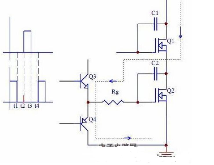
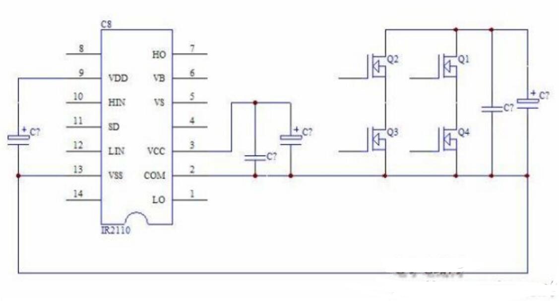
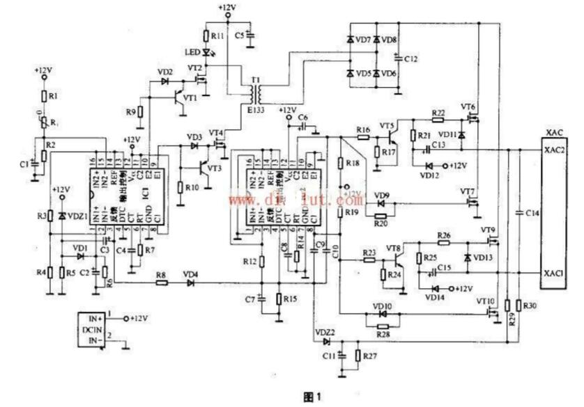
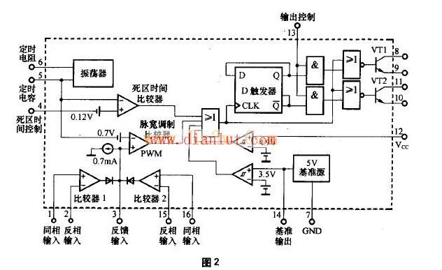
In C1 and C2, the GD junction capacitance of Q1 and Q2 are respectively, and the upper and lower waveforms of the left side are the gate drive waveforms of Q1 and Q2, respectively. We start from the t1-t2 dead zone time. It can be seen from the figure that this time is the dead time, that is to say, the two pipes are not conducting during this time, and the midpoint voltage of the half bridge is half of the bus voltage. That is to say, C1, C2 charging is also half of the bus voltage. When the driving signal runs to time t2, the gate of Q1 becomes high level, Q1 starts to conduct, the potential of the midpoint of the half bridge rises sharply, C2 is charged by the bus voltage, and the charging current passes through the driving resistor Rg and the discharge circuit of the driving circuit. Q4, this charging current will generate a glitch voltage on the driving resistor Rg and the driving circuit discharge tube Q4, please see the red vertical line at time t2 in the figure. If the magnitude of this glitch voltage exceeds the Q2 turn-on voltage Qth, the upper and lower tubes of the half bridge are common. Sometimes the upper and lower tubes are slightly common and do not necessarily explode, but the power tube will be heated. Observing the oscilloscope on the busbar will also see obvious interference burrs. Explosion is only possible when the common cause is serious. Another feature is that the higher the bus voltage, the higher the glitch voltage, and the more the fuse will be caused. The logic ground of pin 13 and the driving ground of pin 2 should be separated when routing. Generally, it should be connected to the negative terminal of 5V filter capacitor and then to the negative terminal of high-voltage filter capacitor. The drive ground should be connected to 12-15V. Drive the negative terminal of the filter capacitor of the power supply to the source of the MOS farther away from the two low-side high-voltage MOS transistors. As shown below: In a sine wave inverter, because the carrier frequency is higher, the bus voltage is also higher, and the bootstrap diode uses a high frequency and high voltage diode. Since the carrier duty ratio is close to 100%, the capacity of the bootstrap capacitor is calculated according to the fundamental wave, and it is generally required to take 47-100uF, preferably a small high-frequency capacitor. In the circuit of Fig. 1, the chip IC1 and its peripheral circuits, the transistors VT1, VT3, the MOS power transistors VT2, VT4 and the transformer T1 form an inverter circuit of 12V DC conversion to 220V/50kHz AC. It is composed of chip IC2 and its peripheral circuits, transistor VT5, VT8, MOS power tube VT6, VT7, VT9, VT10 and 220V/50kHz rectification, filter circuit VD5-VD8, C12, etc. 220V/50kHz high frequency AC conversion to 220V/50Hz The power frequency AC conversion circuit finally outputs 220V / 50Hz AC power through the XAC socket for various portable appliances. In Figure 1, IC1 and IC2 use the TL494CN (or KA7500C) chip to form the core control circuit of the vehicle inverter. TL494CN is a dedicated double-ended switching power supply control chip. Its suffix letter CN indicates that the package shape of the chip is a double-in-line plastic package structure. The operating temperature range is 0°C-70°C, and the limit working power supply voltage is 7V~40V. The maximum operating frequency is 300kHz. In the circuit of Fig. 1, R1 and C1 of the 15-pin peripheral circuit of IC1 constitute a power-on soft-start circuit. At the time of power-on, the voltage across the capacitor C1 is gradually increased from 0V. Only when the voltage across C1 reaches 5V or more, the pulse width modulation circuit inside IC1 is allowed to start working. When the power is turned off, C1 is discharged through the resistor R2 to ensure that the soft start circuit works normally at the next power-on. R1, Rt, and R2 of IC15's 15-pin peripheral circuit form an overheat protection circuit. Rt is a positive temperature coefficient thermistor. The room temperature resistance value can be selected from 150Ω to 300Ω. Appropriate selection can improve the startup of the overheat protection circuit. Sensitivity. Wired Earphones,Waterproof Earbuds,Noise Cancelling Earphones,Gaming Earphones GUANGZHOU LIWEI ELECTRONICS CO.,LTD , https://www.gdliwei.com


High-frequency inverter rear-stage circuit diagram 1: