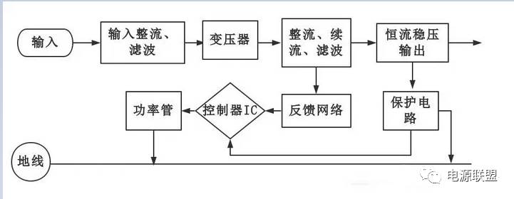
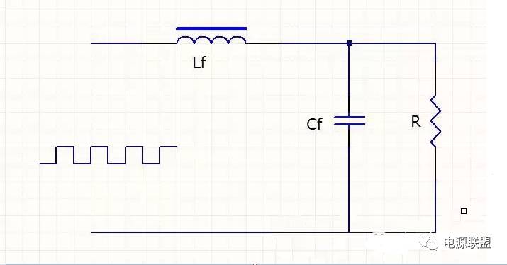
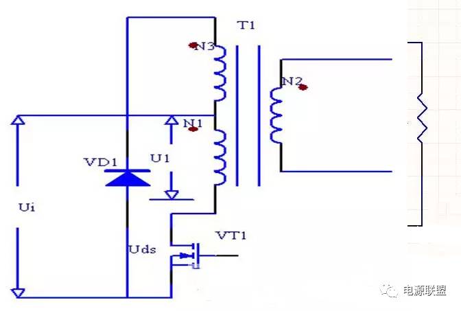
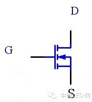
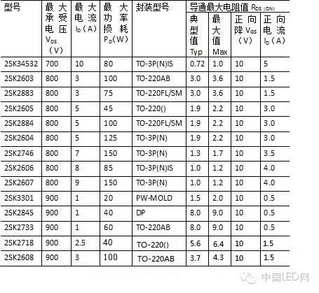
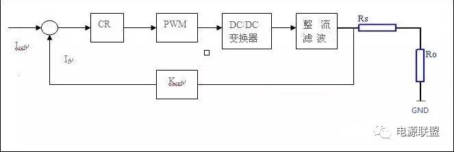
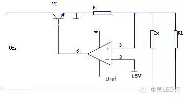
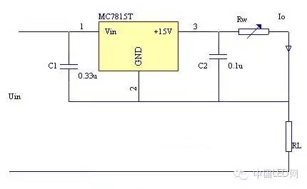
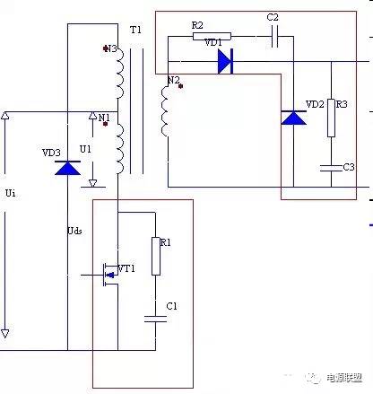
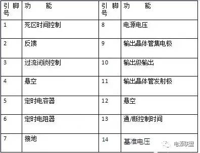
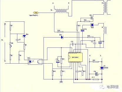
As a new light source for lighting, LED lamps are gradually being applied on a large scale and in a wide range. The core part of determining the performance and life of LED lamps is the LED constant current driving circuit, the life of LED lamps (light attenuation) and The stability of the drive current is related to current ripple or noise. In this paper, taking AC AC power supply to output constant DC DC as an example, several steps must be carried out in the design to get the LED constant current drive power supply design. The first step: clarify the technical requirements of the LED driver flyback power supply We start today with AC-DC with a single-ended forward switching power supply topology, because it is a small, economical, and more switching power supply application, and its power output is most suitable from 50 to 200W. The design technical requirements are as follows: Input voltage: AC 220V ± 10% Ripple voltage UP: 0.5V Output voltage UO: 15V Output ripple current IP: ±0.1A Output current IO: 10A Duty cycle: D max = 0.42 Step 2: LED constant current flyback power supply design steps 1, the overall flow chart Like the switching power supply design, the LED drive flyback power supply is also considered first, and then the power supply is designed separately, followed by the design of the overall and auxiliary functions, and finally the test and design optimization. The following design steps flow: 2. Drive power module function chart The third step: transformer design 1, the output transformer secondary voltage U2 calculation UL is the voltage drop across the secondary winding of the output choke, and Uf is the forward voltage of the output diode. The lowest secondary voltage U2min is: Assume 2, the primary and secondary coil calculation The minimum value of the input DC voltage U1 is calculated using the U1min value calculated by the output circuit. According to China's transmission and distribution situation U1=200~253V, the transformation ratio N is Select EI-30 according to the output capacity core size relationship table 3-4 [2]. Its effective area is S=111mm2. The core material is equivalent to TDK's H7C4, and the maximum working track density Bm can be found from Figure 3-4. The core temperature in actual use is about 100 °C, and Bm, which is 0.3T or less, can be selected to maintain the linear range. When the core temperature is 100 ° C and the operating frequency is 200 KHz, it is reduced by about 0.1 T. According to the coil calculation formula, Thus, the secondary N2 = 4, where Bm is the magnetic flux density (T) of the core; S is the effective cross-sectional area (mm2) of the core. The number of turns in the primary coil is determine. The voltage U2min required for the secondary coil must be sufficient, so a correction calculation of ton max is performed. Then there, The Dmax correction result is 0.42, still in the range of 0.4 to 0.45, and the following calculations can be continued. Step 4: Output Filter Design In the inductor with a magnetic core in the switching power supply, an "L" type filter composed of an inductor Lf and an output filter capacitor Cf is generally used as shown below. The inductor coil exhibits a high inductance against high-frequency components, and the capacitor exhibits a small capacitive reactance to high-frequency components, which has achieved the effect of suppressing ripple and smoothing DC in the circuit. 1. Design of the inductance value of the output choke Calculate the current flowing into the output choke L is the inductance (μH) of the output choke; it is 10%~30% of the output current. Then there is The inductance L value is: It can be seen that a choke of 11.86 μH, 10 A is required. 2. Determination of output filter capacitor The choice of output capacitor depends on how many millivolts the output ripple voltage is controlled. The output ripple voltage is determined according to the equivalent series resistance of the output capacitor, but is generally specified as a range of 0.3% to 0.5% of the output voltage. Another cause In the range of 200HKz, capacitors with a value below 37.5m are required. So you can choose 20V, 8200 H, then 31m, the allowable ripple current is 2.9Ams. The ripple current flowing to the capacitor is: That is 0.58A < 2.9A, indicating that the capacitor is suitable 3, filter resistance design If you are not using the current interrupt of the output choke and use it directly, you can assume the resistance value Rd. Then assume that the resistance Rd power consumption is Wrd Step 5: Reset circuit calculation The reset circuit is as shown. When the switching power tube VT1 is turned on, the magnetic flux of the transformer T1 is increased, and the magnetic energy is stored to T1. When the VT1 is turned off, the excited magnetic energy is released, and the reset coil is turned on the T1 to pass the magnetic energy through the VD1 when the VT1 is turned off. Feedback to the input. Then the magnetic reset is serially connected to the middle diode VD1 of N3 to withstand the maximum voltage. Then choose VD1 rated voltage is 800V, which basically meets the requirements. Step 6: Power switch selection The picture shows a MOSFET type power switch tube, which mainly has a small driving power and a large power capacity of the device; the second remarkable feature is a fast switching speed and a high operating frequency, and his thermal stability is superior to GTR, etc. Widely used switching devices. According to the single-ended forward converter meter, the switch tube VT1 is subjected to the maximum voltage formula: The maximum current flowing through the MOSFET switch is: According to the following power MOSFET table 3.7, the 2SK2718 model can be selected. It has a maximum withstand voltage of 900V, allows a maximum current of 2.5A, and a power loss of 40W, which is the minimum power loss. Step 7: Output diode selection The output diodes are Schottky diodes (SBD), low loss diodes (LLD), and high speed diodes (FRD). Schottky diodes should be used for low voltage and high current, and low loss or trim diodes for others. (1.) When selecting a diode, pay attention to selecting a diode with a reverse recovery time trr. This is because the current flowing back into the diode when the main switching element is closed affects the primary coil switching characteristics and causes the loss to increase. At the same time, the output noise is also greatly affected. Therefore, the general principle of output rectifier diode selection has four points. 1. Select a rectifier diode with a small forward voltage drop VDF; 2. Select the reverse recovery time trr rectifier diode; 3. Select a forward recovery voltage VFRm rectifier diode; 4. Select reverse leakage current IR small rectifier diode. (2.) Freewheeling diode VD2 selection The reverse voltage UVD2 on the freewheeling diode VD2 is the same as the maximum value of the secondary voltage of the output transformer. According to the formula of the single-ended forward converter: The current Ir flowing through it is generally regarded as approximately the same as IO, that is, Ir=Io=10A.. The low-loss diode MBR1545 can be selected as a freewheeling diode with parameters Uds=45V, IO=15A, and trr<1.0ns. The eighth step: constant current output circuit design 1, constant current output principle To achieve constant current function, any power supply needs to detect and sample the output current of the power supply, compare it with the current setting value, that is, the reference value, and adjust it by negative feedback amplification (P, PI, PID). The linear series regulator regulates the voltage drop of the regulator, while the switching power supply regulates the pulse width (or duty cycle) of the converter to maintain a constant output current. The figure below is a diagram of the constant current control feedback system. In the figure, Iref is the current setting reference; CR is the current PI adjustment; Kfi is the current sampling feedback coefficient; RS, Ro is the current sampling resistor and the load resistance. The system adopts current mode control, which can detect the output current of the converter, appropriately select the feedback coefficient Kfi, and realize constant current control through P (proportional), PI (proportional integral), and PID (proportional integral differentiator). Constant current control can also be achieved by changing the voltage or current without changing the feedback coefficient. The following figure is a common circuit for constant current power supply, in which the sampling resistor RS is connected in series in the power loop as a sampling component of the loop current. It converts the loop current into a voltage signal, and compares it with the reference voltage Uref in the amplifier, and then sends it to the base of the adjustment tube VT, and the drive adjustment tube VT compensates for the change of the output current IO. It is possible to achieve constant current output. 2, constant current output calculation The constant current output circuit is a switch constant current source circuit composed of an integrated voltage regulator. The MC7815 is a three-terminal fixed integrated regulator, RL is an LED diode load resistor, and RW is an adjustable resistor. Working principle: The fixed integrated regulator works in a normal state, and a potentiometer RW is connected between the output 2 and the common terminal 3 to form a fixed constant current source. Adjust RW, you can change the current, the output current is Where Iq is the electrostatic flow of MC7815, less than 10mA. When the RW is small and the output current is large, Iq can be ignored. When the voltage or load in the circuit changes, the MC7815 changes its own voltage difference to maintain the current through the load. When RW=1~15, then it outputs a constant current variation range. Therefore, 10A constant current output can be achieved. The ninth step: buffer absorption circuit design In the switching power supply, due to the leakage inductance of the transformer, the lead inductance of the wiring, and the switching tube, a high voltage spike is generated at the moment of turning off. Rectified Fast Recovery Diodes Due to the memory effect, high reverse recovery rolling spikes can also occur during reverse recovery. The occurrence of these overvoltage spikes not only jeopardizes the operational safety of power devices, but also creates strong electromagnetic interference noise. To do this, a spike voltage snubber circuit must be designed across the power device. The buffer circuit diagram is shown in the red box in the figure: There are capacitor components in the snubber circuit. The terminal voltage of the capacitor cannot be abrupt. When the MOSFET power switch is turned off, a spike voltage is formed. The pulse energy is transferred to the capacitor for storage, and then the energy storage of the capacitor is consumed by the resistor or returned to the power source to buffer. Absorbs the voltage tip. The reverse surge voltage generated across the output diode is also limited, so that the reverse surge current is reduced, as well as reduced losses and possible oscillations. The tenth step control circuit design The following is the μPC1094C control circuit 1, the oscillator The oscillation frequency fosc of the oscillator is determined by a timing resistor R17 connected to pin 6 and a timing capacitor C15 connected to pin 5. The oscillation frequency at that time. 2, start circuit The startup circuit is connected to the external power supply of R14 on pin 8 to provide Vcc=15V power supply for the chip operation, and connected to pin 9 is connected to the external circuit to provide the collector voltage through R10. 3, current limiting circuit The overcurrent protection circuit consists of R18, R19, and C16. They are connected to pin 3, and under normal conditions, the voltage on pin 3 is less than 200mV. When an overcurrent occurs, the voltage on pin 3 exceeds the positive and negative threshold of 200mV, and the output stage is locked low. Before the next pulse period, the overcurrent latch resets and the overcurrent of the next cycle is performed. Detect, limit the pulse width. 4, over voltage protection circuit The overvoltage protection circuit is composed of photocouplers PC1 and R16. When the output voltage exceeds 15V, the photocoupler PC1 operates, and the feedback voltage circuit is connected through the pin 2 to lock the output stage to a low level. 5, the maximum duty cycle setting and soft start The maximum duty cycle is determined by the voltage divider ratio of resistors R14 and R15. In order to prevent the magnetic saturation of the transformer, When the power supply voltage is just started, the voltage on capacitor C14 in parallel with R14 cannot be abrupt, the voltage on pin 1 is UREF, and the duty ratio is the largest. 6, the output voltage control circuit The output voltage can be determined by adjusting the voltage divider circuit consisting of R5, R6 and R7: The eleventh step: PCB wiring When drawing PCB layout, you should first determine the location of the components, then arrange the ground wire, power cable, and then arrange high speed. Signal line, and finally consider the low speed signal line [8]. The position of the components should be grouped according to the power supply voltage, digital and analog circuits, speed, current, etc., to avoid mutual interference. The location of the pattern components determines the placement of the individual pins of the PCB connector. All connectors should be placed on one side of the PCB, avoiding cables from both sides and reducing common mode emissions. 1, the power supply Under consideration of safety conditions, the power line should be as close to the ground as possible, reducing the ring area of ​​the differential mode radiation, and also helping to reduce the crosstalk of the circuit. 2, clock line, signal line and ground line position The signal line is close to the ground line, and the ring area formed is small; this is reasonable. 3, divided by logical speed When fast, medium, and low-speed logic circuits need to be placed on a board, high-speed devices should be placed close to the edge connector, while low-speed logic and memory should be placed away from the connector. This is advantageous for the reduction of common impedance coupling, radiation and crosstalk. 4, should avoid PCB wire discontinuity 1), the trace width should not be abrupt; 2), do not suddenly corner the wire. The above several design steps are the general steps for designing an LED constant current driving power supply, which is introduced here today.
A TPU Screen Protector made of the super toughness of the honeycomb structure. Its unique ultra-soft properties allow it to cover the most complex curves and contours in a device.
Srceen Protector For Xiaomi,Hydrogel Screen Protector For Xiaomi,TPU Screen Protector For Xiaomi,Hydrogel Film for Xiaomi Shenzhen Jianjiantong Technology Co., Ltd. , https://www.jjttpucuttingplotter.com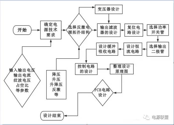











The self-healing design of the Hydrogel Screen Protector can protect the display screen of the device from damage, leave no air bubbles, and maintain the sensitivity of the touch screen. Advanced anti-fingerprint and dust- and oleophobic overlays keep your screen smudge- and dirt-free. This overlay is also important in providing maximum touch sensitivity for improved high-speed glide and optimal touch response.
The optical transparency of the Hydrogel Film is more than 90%, showing you the most original screen color and bringing the most realistic visual experience.
If you want to know more about the product information of the Hydrogel Screen Protector for Xiaomi, please click the product details to view the parameters, model, picture, price and other information of the Xiaomi Screen Protector.
Whether you are a group or an individual, we will do our best to provide you with accurate and comprehensive information about Hydrogel Screen Protectors!