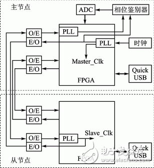
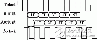
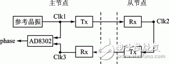
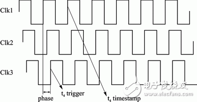
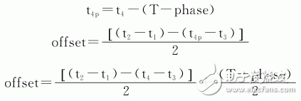
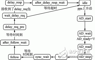
Abstract : The principle of the Precision Clock Synchronization Protocol (PTP) is introduced. This paper simplifies the protocol and designs and implements a low-cost, high-precision clock synchronization system solution. In this scheme, functions such as local clock unit, clock protocol module, transmit buffer, receive buffer, and system time stamp are implemented in the FPGA. After testing, the program can achieve ns-level synchronization accuracy. The solution is low cost and easy to expand, making it ideal for LAN clock synchronization applications. Clock synchronization technology plays a pivotal role in many large-scale physics experiments and industrial applications. For example, in the Jinping dark matter detection experiment in Sichuan, China, it is necessary to provide corresponding time information for a plurality of independent detection devices, including a central detector (HpGe), a liquid argon anti-conformity detector, and an external cosmic ray anti-coincidence detection in the laboratory. [1]. For example, in the Daya Bay neutrino experiment, it is necessary to provide synchronized clocks and time stamps for the sub-detectors of the three experimental halls, as well as to provide synchronized clocks and time stamps for future long-baseline neutrino oscillation experiments [2]. To this end, this paper designs a set of high-precision, low-cost, easy-to-expand time-stamp synchronization system based on programmable logic device FPGA. 1 Introduction to PTP Protocol Five types of transport messages [3] are defined in the IEEE 1588 protocol: synchronous message (sync), follow message (follow_up), delayed request message (delay_req), delayed response message (delay_resp), and management. Message (management). The first four types of packets are mainly used for time stamp exchange. The process of specific time stamp exchange is shown in Figure 1. Figure 1 Schematic diagram of the PTP protocol synchronization process As shown in FIG. 1, the timestamp synchronization process includes a master node and a slave node, both of which use a crystal oscillator to maintain a local clock. The purpose of synchronization is to synchronize the timestamp of the slave's local clock with the timestamp of the master's local clock. When not synchronized, the slave node has a time offset offset from the master node. The process of synchronization can calculate this deviation. The master clock periodically sends a synchronization message SYNC to the slave clock. There is no valid data in this message, but when SYNC is issued, the master node can record the timestamp t1. When the slave node receives the SYNC, the slave node can record it. Timestamp t2. In order for the slave node to also know t1, the master node then sends a follow message FOLLOW_UP to the slave node, which contains the valid data of t1. Then, in order to calculate the delay from the master node to the slave node, the slave node sends a DELAY_REQ message to the master node for a period of time after receiving the FOLLOW_UP from the node. Similar to SYNC, when DELAY_REQ leaves, the timestamp t3 is obtained. When DELAY_REQ reaches the master node, the master node gets the timestamp t4. After a period of time, the master node sends a DELAY_RESP message to the slave node. This message contains t4, so that four timestamps t1~t4 are obtained from the node. After the above four timestamps, assuming that the master node to the slave node and the slave node to the master node transmit and the network delay is unchanged, the calculation method of the transmission delay and the clock offset can be obtained: If the PTP master-slave link is symmetric, that is, Dm2s=Ds2m=delay, then: It can be known from the above analysis method that whether the link of the PTP master-slave node is symmetric or not will affect the calculation of the offset, thereby affecting the synchronization precision of the time stamp. In addition, the local and slave nodes need to maintain the local clock with a local crystal. As time goes by, the crystal oscillator has a frequency drift, and the natural frequencies of different crystal oscillators also have deviations. These two properties will affect the accuracy of clock synchronization. In order to achieve high-precision time synchronization, the synchronization system should be designed with both the symmetry of the master-slave link and the characteristics of the crystal oscillator. 2 The overall structural design of the electronic design clock synchronization system is shown in Figure 2. Figure 2 Hardware structure diagram of the clock synchronization system In this scheme, the master node and the slave node use the same hardware circuit. At the time of design, a jumper is designed on the hardware circuit board, and a hardware circuit can be selected as the master node or the slave node. In order to ensure the link symmetry of the master-slave node, the clock transmission and reception path of the PCB board and the length of the PTP packet transmission and reception path should be designed with a serpentine line to ensure the same length. In addition, in order to eliminate the influence of the frequency drift of the crystal oscillator and the frequency deviation, in this scheme, the slave node does not use the local crystal oscillator, but directly uses the clock signal transmitted by the master node as the time stamp, that is, the master node and the slave node. A homologous clock is used. Although the local clock used by the master-slave node is homologous, the clock of the master-slave node is phase-difference due to the difference in the transmission path of the clock. This phase difference, if not considered in the design, can seriously affect the synchronization accuracy that can be achieved by the entire clock system. As shown in FIG. 3, if the phase difference of the local clock of the master and slave nodes is not considered in the system, that is, the phase in the figure, the synchronization precision that the clock system can achieve is preferably the value of the phase difference. Assume that the master-slave node has a period T of 100 ns and the master-slave node has a phase difference of 60 ns, which means that the highest precision that the synchronous system can achieve is 60 ns. Figure 3 Schematic diagram of the importance of the clock phase difference measurement of the master-slave node In order to further improve the accuracy of time stamp synchronization, the phase measurement module must be designed to eliminate the influence of the master-slave clock phase difference on the synchronization accuracy of the time stamp. Therefore, the master node includes a phase discrimination chip and an ADC chip for accurately measuring the clock phase difference of the master-slave node time stamp. With this phase difference measurement module, can it really eliminate the influence of the clock phase difference of the master-slave node timestamp? The answer is yes. Figure 4 is a schematic diagram of the master-slave clock propagation. The AD8302 is the phase discrimination chip used in this paper. Figure 4 Schematic diagram of master-slave node clock propagation We already know that in order to achieve accurate synchronization of the timestamps of the slave node and the master node, the most straightforward method is to calculate the offset value as accurate as possible, that is, to obtain the value of t1 to t4 as accurate as possible. In Figure 4, Clk1 is the master node crystal clock, and Clk2 is the slave node receiving the clock from the master node. Because of a long propagation path, Clk2 has a phase difference with respect to Clk1. In order to measure the phase difference at the master node, Clk3 is the clock obtained by the slave node transmitting Clk2 directly to the master node, and thus Clk3 has a phase difference with respect to Clk2. A schematic diagram of specific Clk1 to Clk3 is shown in FIG. 5. Figure 5 master-slave node clock diagram For the timestamp t1, t1 refers to the time when the SYNC packet is sent from the master node, the trigger clock is Clk1, and the timestamp clock is the master node's system clock Clk1, so t1 is accurate. For the timestamp t2, t2 refers to the time when the SYNC packet arrives at the slave node, the trigger clock is Clk2, and the timestamp clock is the slave system clock Clk2, so t2 is also accurate. For the timestamp t3, t3 refers to the time when the DELAY_REQ packet is triggered from the slave node, the trigger clock is Clk2, and the timestamp clock is the slave system clock Clk2, and thus t3 is also accurate. For the timestamp t4, t4 refers to the time when the DELAY_REQ packet arrives at the master node, the trigger clock is Clk3, and the timestamp clock is the system clock Clk1 of the master node, and thus t4 is not accurate and is biased. From the clock diagram of Figure 5, the exact t4p should be before t4: It can be seen that the phase difference measurement module takes a significant role in the entire time stamp synchronization scheme. 3 firmware programming Figure 6 Block diagram of the main node firmware structure Figure 7 is a state machine transition diagram of the master node clock synchronization protocol module. Figure 7 State machine conversion diagram of the master node synchronization protocol module In the idle state, when the rising edge of the pps signal is detected, the entire synchronization cycle begins. First, start the ADC read operation. When AD_ready='1' is reached, the ADC data is ready and then read and saved. Then, it enters the sync state. In this state, the master node sends a SYNC synchronization packet to the slave node, after which the module enters the sync_wait state. After a fixed period of time, the module enters the follow state, in which the master node sends a FOLLOW_UP synchronization packet to the slave node. After the module enters after_follow_wait, after waiting for a fixed period of time, the module enters delay_req_pre. In this state, the master node will notify the slave node to send the DELAY_REQ packet. After that, the module waits for the DELAY_REQ packet. If the DELAY_REQ packet is not waited for a long time, that is, waiting for timeout, the module returns the idle state; if the DELAY_REQ packet is received, the master node sends DELAY_RESP to the slave node. Finally, after waiting for a while, the module returns to the idle state. 3.2 Slave Firmware Design The block diagram of the node firmware is shown in Figure 8. The phase part calculation module is used to calculate the phase value mentioned above. The function of the offset calculation module is to calculate the exact offset using t1~t4 and phase values. value. The primary role of the slave clock synchronization protocol is to control the transmission and reception of messages and to update the local clock. Figure 8 slave node firmware block diagram Figure 9 is a state machine transition diagram of the slave node clock synchronization protocol module. Figure 9 State machine conversion diagram of the slave node clock synchronization protocol module When in the idle state, the slave node monitors the received data stream until it reaches the wait_follow state immediately after detecting the sync packet. In the wait_follow state, the slave node also monitors the received data stream until the last_up packet is detected, and immediately enters the wait_pre state. If the follow_pre packet is not received for a long time in this state, it will wait for the timeout to return to the idle state. Similarly, in the wait_pre state, until the delay_req_pre packet is detected, it jumps into the delay_req state; if it waits for a timeout, it returns the idle state. In the delay_req state, the slave node sends the delay_req packet to the master node and immediately enters the wait_delay_resp state. In the wait_delay_resp state, after the delay_resp packet is detected, the slave node immediately enters the phase_cacul state; if the delay_resp packet is not detected for a long time, the idle state is returned. In the phase_cacul state, after the phase difference calculation module is started, the wait_phase_result state is immediately entered. In the wait_phase_result state, after the phase measurement result is ready, the delay_cacul state is entered; if the phase result is not ready for a long time, or the phase result is wrong, the idle state is returned. In the delay_cacul state, after the offset calculation module is turned on, the wait_result state is entered. In the wait_result state, when the offset measurement result is detected, the offset_update state is entered; otherwise, it returns to the idle state. In the offset_update state, the offset correction signal is sent from the node clock synchronization protocol to the local clock module, thereby updating the local clock of the slave node and then entering the idle state. 4 Test Results The actual test environment consists of a master node and a slave node, connected by fiber optics. The oscilloscope is used to observe the pps signal output by the master node and the slave node. Since the clock phases of the master and slave nodes are inconsistent, the oscilloscope observes this phase difference. When the rising edge of pps comes, the time stamp of the master and slave nodes is output to the PC through the serial port module. By comparing the master-slave phase difference measured by the oscilloscope with the difference between the master-slave timestamp and the pps rising edge, the true timestamp synchronization accuracy can be obtained. In this test, three different lengths (3 m, 6 m, 5.15 m) of fiber were used, and then the experimental results under different lengths of fiber were observed to determine the accuracy of the clock synchronization system. The master-slave node phase difference histogram and the corresponding time-stamp difference histogram are slightly omitted. From the results of these three different lengths of fiber, the time synchronization accuracy of the synchronous clock system implemented in this paper can reach 1 ns. Conclusion The clock synchronization system implemented by this scheme is based on the time-based message communication in the IEEE 1588 protocol and is implemented in a pure hardware circuit (FPGA). By adding a phase difference test module to the master node, the influence of the phase difference of the master and slave nodes is eliminated, and the timestamp synchronization accuracy achieved last is as high as 1 ns. The clock synchronization system designed in this paper requires low cost and high synchronization precision, which is very suitable for applications where high-precision time stamping is required.
recordable stuffed toy:
Ningbo AST Industry Co.,Ltd has 17 Years Experiences to produce the Recordable Plush Toy,Stuffed toy,Teddy Bear,Soft
Toys ,Musical Plush toys and so on ,we can assure you of competive
price,high quality,prompt delivery and technology supporting.
1. recordable stuffed toy application :
The Recordable Plush Toys as the Gifts can record your own and present them to your friends,children and family.
USA, UK,Canada,Germany, Turkey,Russia,Poland,Switzerland,Netherland
,Frence Hungary ,Australia,New Zealand, Brazil,
Columbia,Argentina,Thainland,Singapore , Malaysia and so on
Recordable Plush Toy, Musical Teddy Bear, Recordable Stuffed Toy AST Industry Co.,LTD , https://www.astsoundchip.com
The PTP Precision Clock Timing Protocol is also known as the IEEE 1588 protocol. Its basic function is to use time-based message communication methods to keep all clocks in a distributed network accurately synchronized with a specific clock. The IEEE 1588 protocol can be implemented in software or in specialized hardware. Obviously, hardware implementation can achieve higher precision. The synchronization system in this article is based on pure hardware implementation. 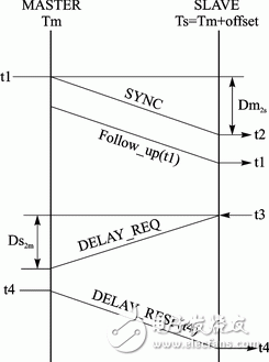
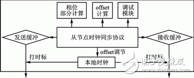
3.1 Master node firmware design The firmware structure block diagram of the master node is shown in Figure 6. The A/D control module and phase measurement module are used to control the amplitude phase discrimination chip and the ADC chip. The function of the sending buffer is to send the communication message in the master node clock synchronization protocol in Manchester coding mode. The function of the receiving buffer is to decode the corresponding communication message from the receiving path. The role of the local clock module is to maintain a local clock. The main function of the master node clock synchronization protocol is to control the transmission and reception of packets. 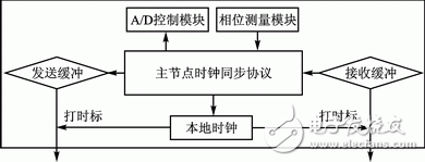
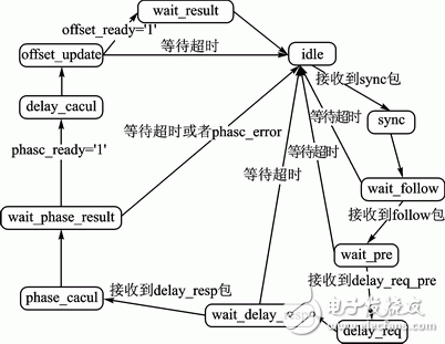
2.Press the Record Button to record your Own Message,then press the play button to play the message.
3.Recording time:12s,20s,30s and so on
4.Sound Quality:Clearly and Loudly
5.Packaging;Color box
6.Certification:CE ,Rohs
7.Export to:

