Each transceiver has an independent sending end, the sending end is composed of PMA (Physical Media Attachment, physical media adaptation layer) and PCS (Physical Coding Sublayer, physical coding sublayer), where the PMA sublayer contains high-speed serial-parallel conversion ( Serdes), pre / post-emphasis, receiving equalization, clock generator and clock recovery circuit. The PCS sublayer contains 8B / 10B codec, buffer, channel binding and clock correction circuits. For the sending end of GTX, the structure is shown in Figure 1.
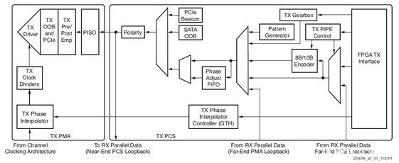
figure 1
FPGA internal parallel data enters the TX transmitter through the FPGA TX Interface, and then is processed by the various functional circuits of the PCS and PMA sublayers. Finally, it is output as high-speed serial data from the TX driver. The following will introduce each functional circuit.
FPGA TX Interface (TX user interface): TX Interface is the interface that user data is sent to GTX. The signals of this interface are shown in Table 1.
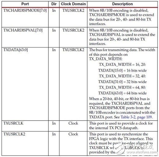
Table 1
The transmit data interface is TXDATA, the sampling clock is TXUSRCLK2, and TXDATA is sampled on the rising edge of TXUSRCLK2. The rate of TXUSRCLK2 is determined by the line rate, the bit width of the TX Interface interface and whether 8B / 10B is enabled (TXUSRCLK2 frequency = line rate / TX_DATA_WIDTH; for example, if the line rate is 10Gb / s and TX_DATA_WHDTH is equal to 80, then the frequency of TXUSRCLK2 is 125MHz). The bit width of TXDATA can be configured as 16/20/32/40/64/80 bit width. Through the three attribute settings of TX_DATA_WIDTH, TX_INT_DATAWIDTH and TX8B10BEN, it can be configured into different bit widths. The specific attributes are shown in Table 2.
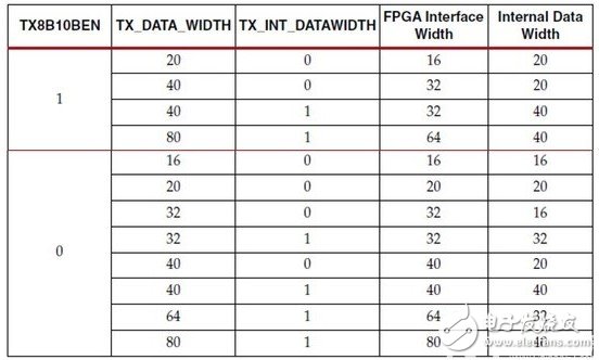
Table 2
GTX's TX Interface is divided into internal data bit width and FPGA interface bit width, where internal data belongs to the TXUSRCLK clock domain, FPGA interface data belongs to the TXUSRCLK2 clock domain, and internal data bit width supports 2byte / 4byte, FPGA interface data bit width supports 2byte / 4byte / 8byte, therefore, it is determined that TXUSRCLK and TXUSRCLK2 have a certain clock multiple relationship. The clock multiple relationship between TXUSRCLK and TXUSRCLK2 is shown in Table 3, where the TX_INT_DATAWIDTH attribute is set to "0", indicating that the internal data bit width is 2byte, if Set to "1", it means that the internal data bit width is 4byte (when the line rate is greater than 6.6Gb / s, it should be set to "1").

table 3
The TXUSRLK and TXUSRCLK2 clocks are related, and the following two guidelines should be followed when clocking these two clocks:
1. TXUSRCLK and TXUSRCLK2 must be aligned on the rising edge, the smaller the deviation, the better, so you should use BUFGs or BUFRs to drive these two clocks (because there is no phase correction circuit or FIFO between the TX Interface and the PCS sublayer, so strict Align, my own understanding).
2. Even if the reference clocks of TXUSRCLK, TXUSRCLK2, and GTX run at different clock frequencies, it must be ensured that the three must use the same-origin clock.
Clock structure at the sending end: In order to better understand how the sending end of the GTX works, it is necessary to understand the clock structure at the sending end. Figure 2 is a diagram of the clock structure at the sending end.
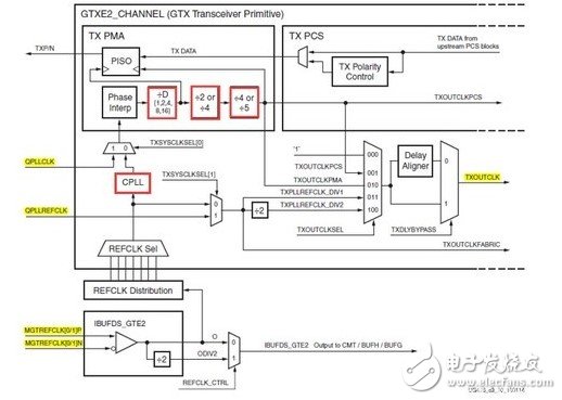
figure 2
The content in the red frame and the yellow background is what we need to understand. The MGTREFCLK in the figure is the reference clock of GTX mentioned in the previous article. After an IBUFDS_GTE2 source language, it enters GTX to drive CPLL or QPLL. . For TX PMA, the main function is parallel-to-serial conversion. The clock for parallel-to-serial conversion can be provided by CPLL or QPLL, which is selected by TXSYSCLKSEL. There are three red boxes in the TX PMA sublayer. And the parallel clock divider, the role is to generate a parallel data drive clock, of which the D divider is mainly used to divide the output of the PLL to support lower line rates.
The option ÷ 2 / ÷ 4 is determined by TX_INT_DATAWIDTH. If TX_INT_DATAWIDTH is "0", select ÷ 2, otherwise select ÷ 4.
For ÷ 4 / ÷ 5, it is determined by TX_DATA_WIDTH. If the bit width is 16/32/64, select ÷ 4. If the bit width is 20/40/80, select ÷ 5.
For who drives TXUSRCLK and TXUSRCLK2, the official recommendation is to use TXOUTCLK, which can simplify the design and stabilize at the same time. How to use TXOUTCLK as the driving clock for TXUSRCLK and TXUSRCLK2 Figure 3 shows the driving mode of TXUSRCLK = TXUSRCLK2, Figure 4 shows the driving mode of TXUSRCLK = 2 * TXUSRCLK2.
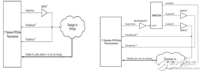
Figure 3 Figure 4
For Figure 4, the value of CLKOUT0 is twice that of CLKOUT1.
TX 8B / 10B Encoder: The transmitting end of high-speed transceiver generally has 8b / 10b encoder. The purpose is to ensure that the data has sufficient switching to provide the clock recovery circuit, the encoder also provides a method to align the data to the word, while the line can maintain a good DC balance. In GTX applications, if the D code is sent, TXCHARISK needs to be pulled low, if it is a K code, the corresponding TXCHARISK will be pulled high.
TX Buffer: To understand the role of the TX Buffer sent, you must first figure out the clock domain of the TX transmitter. The clock domain of the TX transmitter is shown in Figure 5.
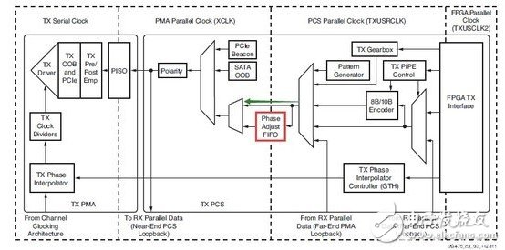
Figure 5
The red box in Figure 5 is the TX Buffer. We all know that the FIFO has the function of isolating the clock domain. Here is no exception. We can know from the figure that the TX Buffer is connected to two different clock domains XCLK and TXUSRCLK. The PCS sublayer at the end contains two clock domains, XCLK (PMA parallel clock domain) TXUSRCLK clock domain. For the stability of data transmission, XCLK and TXUSRCLK must be rate matching, the phase difference can be eliminated, TX Buffer is mainly used to match the two clocks Domain rate and eliminate the phase difference between the two clock domains.
TX Buffer can also be bypassed. The TX transmitter provides a phase alignment circuit to solve the phase difference between the XCLK and TXUSRCLK clock domains, but TX_XCLK_SEL needs to be set to "TXUSR" to keep the XCLK clock domain and TXUSRCLK at the same frequency.
TX Pattern Generator: GTX has a pseudo-random number sequence generation circuit. The pseudo-random number sequence is seemingly random, but it is a regular periodic binary sequence, with good randomness and close to white noise correlation function, so the pseudo-random number sequence can Used for bit error rate measurement, time delay measurement, noise generator, communication encryption and spread spectrum communication, etc., can be used to test the bit error rate of high-speed serial channel transmission in GTX. Circuit.
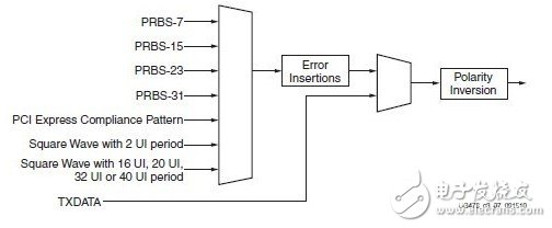
Figure 6
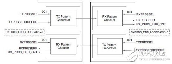
The PRBS generation circuit can be enabled or bypassed. If bypassed, TXDATA will be transmitted to the PMA at the sending end. The PRBS mode test model is generally shown in Figure 7.
Picture 7
TX Polarity Control: The TX transmitter supports the polarity control of the data sent by TX. The coded data output from the PCS sublayer is reversed before entering the PISO serialization. This part of the function is mainly used to compensate for PCB design errors. If you accidentally cross-connect TXP and TXN during PCB design, you can reverse the signal polarity by setting TXPOLARITY to "1".
CHENGRONG travel Portable Laptop Stand is a Laptop Foldable Laptop Stand which you can fold and carry easly in your backpack or briefcase you can use It to change angle of your laptop.
Shenzhen Chengrong Technology Co.ltd is a high-quality enterprise specializing in metal stamping and CNC production for 12 years. The company mainly aims at the R&D, production and sales of Notebook Laptop Stands and Mobile Phone Stands. From the mold design and processing to machining and product surface oxidation, spraying treatment etc ,integration can fully meet the various processing needs of customers. Have a complete and scientific quality management system, strength and product quality are recognized and trusted by the industry, to meet changing economic and social needs .
Computer Stand Riser,Mesh Monitor Stand Riser,Gold Monitor Stand Riser,Shelf Monitor Stand Riser
Shenzhen ChengRong Technology Co.,Ltd. , https://www.laptopstandsupplier.com