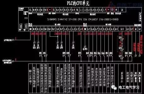
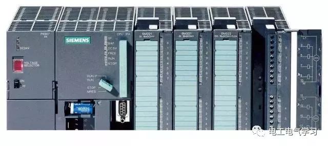
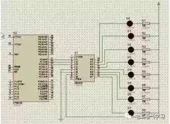
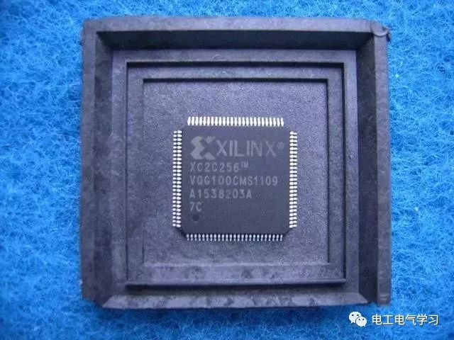
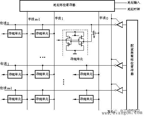
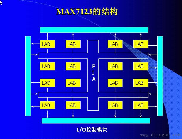
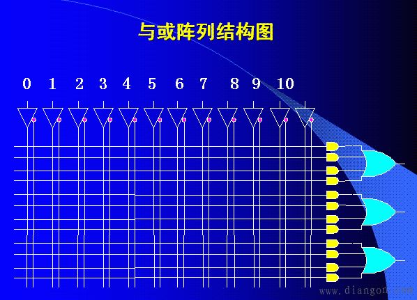
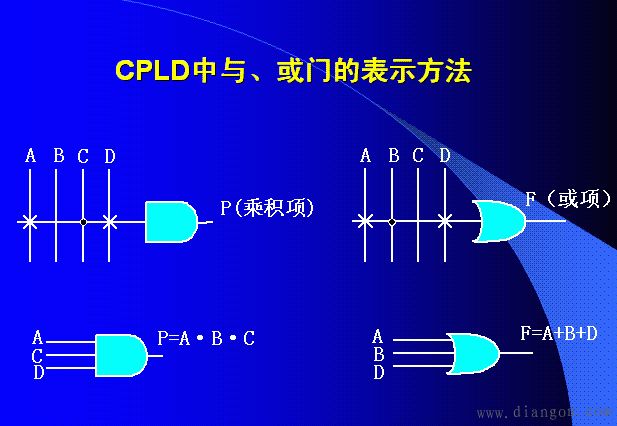
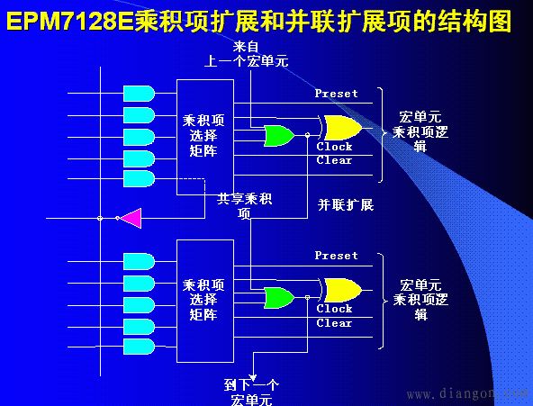
PLC and PLD are not unfamiliar terms for most friends in the control industry and microcontroller enthusiasts. But do you understand their "one word difference"? If you are interested in it, please take a look at what the editor introduced today. 1. Programmable controller (PLC) is a member of the computer family, designed and manufactured for industrial control applications. Early programmable controllers are called programmable logic controllers, or PLCs for short, which are mainly used to replace relays to achieve logic control. With the development of technology, the function of this device has greatly exceeded the scope of logic control. Therefore, today this device is called a programmable controller, or PC for short. However, in order to avoid confusion with the abbreviation of personal computer, the programmable controller is abbreviated as PLC (Programmable Logic Controller). The internal circuit of a certain PLC The main features of PLC PLC function Logic control, timing control, count control, step (sequence) control PID control Data control: PLC has data processing capability. Communication and networking Other: PLC also has many special function modules, which are suitable for various special control requirements, such as: positioning control module, CRT module. A type of PLC control cabinet 2. PLD is the abbreviation of Programmable Logic Device (ProgramableLogicDevice), FPGA is the abbreviation of Field Programmable Gate Array (FieldProgramableGateArray), the functions of the two are basically the same, but the implementation principle is slightly different, so we can sometimes ignore the two. The difference is collectively called a programmable logic device or PLD / FPGA. PLD is the most dynamic and promising technology in the field of electronic design. Its influence is no less than the invention and use of single-chip microcomputers in the 1970s. What can PLD do? It is no exaggeration to say that PLD can complete the functions of any digital device, from high-performance CPU to the simple 74 circuit, which can be implemented with PLD. PLD is like a piece of blank paper or a pile of wood. Engineers can freely design a digital system through traditional schematic input methods or hardware description languages. Through software simulation, we can verify the correctness of the design in advance. After the PCB is completed, you can also use the PLD's online modification capabilities to modify the design at any time without having to change the hardware circuit. Using PLD to develop digital circuits can greatly shorten design time, reduce PCB area, and improve system reliability. Internal circuit of a model of PLD A typical PLD consists of an AND gate and an OR gate array, and any combinational logic can be described with an AND OR expression. Therefore, PLD can complete a large amount of combinational logic in the form of a product sum Function. The products at this stage mainly include PAL (Programmable Array Logic) and GAL (General Array Logic). For programmable logic devices, designers can use low-cost software tools to quickly develop, simulate, and test their designs. Then, you can quickly program the design into the device and immediately test the design in the actual running circuit. The PLD device used in the prototype is exactly the same as the PLD used in the formal production of the final equipment (such as a network router, DSL modem, DVD player, or car navigation system). This eliminates the cost of NRE and the final design is completed faster than when using custom fixed logic devices. Another key advantage of using PLD is that customers can modify the circuit as needed during the design phase until they are satisfied with the design work. This is because PLD is based on rewritable memory technology-to change the design, simply reprogram the device. Once the design is completed, the customer can immediately put into production, only need to use the final software design file to simply program the required number of PLD. Appearance of a model PLD The following uses FPGA as an example to introduce the programming principle of PLD. The programming data storage units are distributed in FPGA in the form of an array, and the structure of the programming data storage unit array is shown in FIG. 1. The storage unit is a 5-tube SRAM structure with only one bit line. Among them, the T tube is the control gate of the unit, which is controlled by the word line. The data is shifted into the shift register in a serial manner, and the address shift register sequentially selects a word line of the memory cell. When the word line of a column is high, the T tube of the column of memory cells is turned on, thereby connecting with the bit line Under the control of the write signal, the data of one word in the data shift register is written into the column memory cell through each column bit line. The programming data is composed into a data stream according to a certain data structure and loaded into the FPGA. The programming data stream is automatically generated by the development software. The development software converts the design into a netlist file, which automatically partitions, places and routes the logic circuit and verifies the design of the FPGA, then generates a programming data stream in the PROM format and forms a programming data file, and finally saves the programming data file PROM. Figure 1 Programming data storage cell array structure At present, all PLD devices that exceed a certain integration level (such as more than 1000 gates) are generally called CPLDs. CPLD consists of programmable logic function blocks around a programmable interconnect matrix. The interconnection between logic units is realized by fixed-length metal wires, and the number and functions of I / O control modules are increased. The basic structure of CPLD can be seen as composed of three parts: programmable logic array (LAB), programmable I / O control module and programmable internal wiring (PIA). MAX7123 structure 1). Programmable logic array (LAB) The programmable logic array is composed of several programmable logic macro cells (Logic Macro Cells, LMC). The internal LMC mainly includes circuits such as arrays, OR arrays, programmable triggers and multiplexers. Can be independently configured for timing or combined working mode. AND OR array structure diagram Representation method of AND and OR gate in CPLD (1) Shared structure of product terms In the macro unit of CPLD, if there are many AND terms in the output expression and the corresponding OR gate input is not enough, you can use the programmable switch to switch other or The gate is used in conjunction with it, or the unused product term is provided in each macrocell for use by other macrocells. Structure diagram of EPM7128E product term expansion and parallel expansion term (2) Multi-trigger structure Each output macrocell (OLMC) of early programmable devices has only one flip-flop, and the CPLD macrocell usually contains two or more flip-flops, of which only one trigger and output The output of the remaining flip-flops is not connected to the output terminal, but can be fed back to the array through the corresponding buffer circuit, so as to form a more complicated sequential circuit together with other flip-flops. These internal flip-flops that are not connected to the output are called "buried" flip-flops. This structure can increase its internal resources without increasing the number of pins. (3) Asynchronous clock Early programmable devices can only implement synchronous sequential circuits. The clocks of flip-flops in CPLD devices can work asynchronously. In some devices, the clocks of flip-flops can also be selected through a data selector or a clock network. In addition, the asynchronous clearing and asynchronous setting of the flip-flop in the OLMC can also be controlled by the product term, so it is more flexible to use 2). Programmable I / O unit (IOC) The CPLD's I / O unit (Input / Output Cell, IOC) is the interface part from the internal signal to the I / O pin. Depending on the device and function, the structure of various devices is also different. Since array devices usually have only a few dedicated input terminals, most of the ports are I / O terminals, and the input signals of the system usually need to be latched. Therefore, I / O is often handled as an independent unit. 3). Programmable internal wiring (PIA) The function of the programmable interconnection is to provide an interconnection network between the logic macrocells and between the logic macrocell and the I / O unit. Each logical macrocell receives the signal from the input terminal through the programmable wiring array, and sends the signal of the macrocell to the destination. This interconnection mechanism has great flexibility, it allows to change the internal design without affecting the pin assignment. Summary: The biggest difference between the two is control logic. PLC is a fixed logic device (function is realized by changing software), and PLD is a variable logic device (function is realized by changing internal circuit structure). In addition, PLC is generally used for the weak point driving strong electricity (automation professional friends must know very well), such as the control of large machine tools, the control of manipulators. The PLD is mainly used in the preliminary design work of integrated circuits such as simulation circuits and weak point control. Smd Led,Smd Fnd Display,Smd Led 0603 Display,Smd Led 0805 Display Wuxi Ark Technology Electronic Co.,Ltd. , https://www.arkledcn.com